Scalable High-Density Sensor-to-Memory Architectures: Topology, Automated Ingestion, and In-Memory Bitwise State Processing
A Technical Monograph on Event-Driven Hardware and Firmware Architectures for Constructing and Continuously Processing Multi-Million-Node State Datasets Entirely In-Memory
Author: Mehdi Zahedi, Electronic Engineering Contact: mehdi.zahedi13790@gmail.com
Author's note on independence and provenance: this monograph is independent engineering work, prepared without institutional funding or sponsorship and not submitted under the auspices of any university or company. The four internal design drafts it synthesizes are the author's own earlier, unpublished writing on this architecture. They are not third-party or anonymous sources, and the phrase "source documents/drafts," used throughout, refers to those earlier drafts.
Abstract
This monograph is written for a specific engineering objective: to use the architecture it describes as a platform for in-memory processing, that is, for building and continuously operating on a very large live state dataset (up to 10,616,832 nodes) that resides entirely in on-chip SRAM. On the real-time path the dataset is never written to disk, flash, or a database, and it is updated and evaluated with in-place bitwise operations rather than record-oriented I/O. The physical switch matrix examined throughout is treated, deliberately, as one concrete instance of a more general problem: acquiring a very large, sparsely changing external state space and reflecting it into a host-addressable in-memory representation with minimal latency and minimal CPU overhead, so that everything downstream (event detection, filtering, classification, logging) can run as pure in-memory computation against that representation.
Keeping such a dataset live at multi-million-node scale surfaces constraints that do not appear at smaller scale: cumulative bus capacitance that violates serial-bus electrical specifications; host pin budgets that cannot grow linearly with node count; sequential polling algorithms whose latency grows in direct proportion to dataset size; and, the constraint most specific to the in-memory objective, a naive per-node memory allocation that can exceed the available on-chip SRAM outright. This monograph documents, synthesizes, and critically extends a hardware and firmware architecture that acquires, ingests, and evaluates up to 10,616,832 discrete external state bits while holding state-update latency below roughly one millisecond, host CPU utilization under two percent of a single core, and the entire live dataset within a few megabytes of on-chip SRAM, with no external memory, disk, or database access on the real-time path.
The architecture rests on four decoupled layers, each addressing one part of the in-memory processing pipeline. (1) A physical acquisition layer, built from CY8C9540A 40-bit I/O expanders and 74HC4067 16-channel analog multiplexers, assembles 288×288 sub-matrix modules of 82,944 crosspoints each; this is the sensing front end that generates the raw bits the dataset represents. (2) A bus layer, built from PCA9546AD four-channel I²C switches, segments the shared serial bus into electrically isolated branches, solving address-space exhaustion and capacitive loading together so that acquisition scales without saturating the path into memory. (3) An ingestion layer, built around an NXP i.MX RT crossover microcontroller, uses Enhanced Direct Memory Access (eDMA), DMA-multiplexer hardware triggering, and dual ping-pong SRAM buffers to move raw peripheral state directly into the live dataset without CPU polling; this is the layer that actually constructs the in-memory representation. (4) An algorithmic layer evaluates state changes with bitwise XOR delta extraction and the ARM Cortex Count Leading Zeros (CLZ) instruction, isolating events in effectively constant time regardless of dataset size. This is the layer that processes the dataset once it is resident in memory, and it most directly answers the in-memory processing objective of this monograph.
Across the four source drafts synthesized here, the headline performance claim is consistent. Legacy sequential polling over a 400 kHz I²C Fast-Mode bus needs approximately 6.2 seconds to sweep the 1,990,656-node base dataset and approximately 33.2 seconds to sweep the maximum 10,616,832-node configuration. The proposed interrupt-driven, in-memory delta-scanning pipeline reduces full-dataset event-detection latency to sub-millisecond timeframes, a reported improvement of roughly 6,200× to more than 33,000×, depending on dataset tier. This document reconstructs the mathematical, electrical, and algorithmic reasoning behind those figures, evaluates their internal consistency, and extends the analysis with context on I²C bus history, switch-matrix ghosting theory, DMA architecture, and the wider landscape of in-memory and real-time system design.
Executive System Targets (In-Memory Processing Objective):
| Parameter | Target Value |
|---|---|
| Maximum in-memory dataset density | 10,616,832 addressable state bits across 128 sub-matrices |
| State-update propagation latency | < 0.88 ms, physical event → live in-memory dataset (event-detection only; the full debounced event adds ≈5 ms — see Section 9.3) |
| Host CPU overhead for in-memory processing | < 1.9% on a 500 MHz ARM Cortex-M33-class core |
| Live in-memory dataset footprint | 2.671 MB (53.42% of 5.0 MB total on-chip SRAM) — no external memory on the real-time path |
| Maximum active-segment bus capacitance | < 100 pF per isolated I²C branch (spec limit: 400 pF) |
| Peak system power draw | < 4.2 W across all sub-banks during simultaneous switching |
Methodological Note: Scope of Validation
This monograph is an analytical synthesis, reconciliation, and critical extension of four unpublished internal design drafts. It is not a report of independent, bench-measured results. No physical prototype of the architecture, at any tier from the 24-expander base configuration to the 128-expander maximum, has been built or electrically tested in preparing this document. Every quantitative figure attributed to "the source documents" (the 6.2 s / 33.2 s legacy polling times, the 0.42 ms and 5 ms latency figures reconciled in Section 9.3, the 6,200×–33,200× improvement ratios, the SRAM footprint figures of Chapter 9, and the electrical parameters of Chapters 4–5 and 8) originates in those drafts' own datasheet-based calculations and simulation-level reasoning, not in oscilloscope traces, logic-analyzer captures, or thermal-chamber measurements of constructed hardware. Where this monograph corrects or reconciles a figure (Sections 1.5, 4.4, and 9.3), it does so against independently verifiable published references (component datasheets and the I²C and debounce-characterization literature cited in the References). That is a stronger evidentiary basis than an uncorroborated internal draft, but it remains a check of internal and cross-literature consistency, not a substitute for measurement on built hardware. Readers and reviewers should therefore treat every performance number here as an analytically derived design target: a claim about what the architecture's electrical and algorithmic design implies it should achieve, falsifiable and worth building toward, but not yet a claim about what a physical instance has been measured to do. The deployment roadmap in Section 10.5 reflects this by recommending prototyping at the base tier before any figure in this monograph is treated as a firm specification.
Reading convention: because no figure here comes from hardware, every present-tense performance statement (for example, "the design reaches X") should be read as "the design is calculated to reach X." Where a statement was revised for this reason, the wording says so explicitly.
Framing Note: Why This Monograph Reads the Source Architecture as an In-Memory Processing System
The source design documents describe their subject mainly in the vocabulary of switch-matrix scanning: keys, presses, releases, debounce. That vocabulary is retained wherever it names a specific physical or electrical mechanism (a switch is still a switch, and a debounce filter still filters mechanical bounce), because relabeling settled engineering terms would obscure rather than clarify the design. What changes, chapter by chapter, is the lens: each mechanism is read for what it contributes to building, maintaining, and computing against a live in-memory dataset, rather than for what it contributes to a keyboard or keypad product. Concretely, Chapters 1–5 characterize the acquisition front end that feeds the dataset and the physical and electrical constraints of doing so at multi-million-node scale; Chapters 6 and 9 form the core of the in-memory processing architecture proper, the mechanisms that construct and size the memory-resident dataset; Chapter 7 is the in-memory compute layer that operates directly on it; and Chapter 10 evaluates the architecture against the in-memory processing objective rather than against the human-machine-interface context the original material assumed. Appendix A closes the main text by positioning the design against the processing-in-memory (PIM) and near-memory computing literature, clarifying what kind of in-memory processing architecture this is, and what kind it is not.
A fair question is why the subject should be called an "in-memory processing" architecture at all, rather than, more plainly, an event-driven switch-scanning system whose working dataset happens to reside in SRAM. That description is shorter, uses settled vocabulary, and claims nothing that would need extended defense. The honest answer has two parts. First, on the physics: nothing in Chapters 1–8 changes if the label is dropped. The acquisition topology, bus segmentation, eDMA pipeline, and XOR/CLZ scan are the same system either way, and readers who find the relabeling unpersuasive can set the framing aside and read this document as a monograph on large-scale switch-matrix scanning without losing anything in those chapters. Second, the framing claims less than it may first appear. It does not claim that this design is a PIM architecture in the sense the PIM/PNM/PUM literature gives that term (Appendix A states directly that it is neither PNM nor PUM by that literature's definitions), nor does it claim any novel memory technology or compute-in-memory circuit technique. It asserts only that the system's defining engineering constraint is keeping a multi-million-bit live dataset entirely within on-chip SRAM and computing against it with in-place bitwise operations rather than record-oriented I/O, and that foregrounding this constraint, instead of keyboard ergonomics, makes the memory-footprint and per-word-cost analysis of Chapters 7 and 9 the central engineering result rather than a secondary detail. Whether that reframing earns its own vocabulary, or should be folded back into "a well-optimized event-driven scan system with a memory-footprint budget," is a judgment about emphasis rather than a factual dispute. The "in-memory processing" label is offered as an interpretive lens on an otherwise conventionally describable scanning system, because Chapters 7 and 9 are, in the author's judgment, better organized around it. It is not a claim of a new category of hardware.
Chapter 1 — Introduction & Problem Space
1.1 The Scaling Crisis in High-Density Switch Interfaces
Every system whose purpose is to maintain a live, in-memory representation of a large external state space — a keyboard, an industrial control panel, a telecommunications patch field, a large-format tactile test fixture, or, in the framing this monograph adopts throughout, any sensor front-end feeding a real-time in-memory dataset — must eventually solve the same problem: how does a finite number of microcontroller pins observe an arbitrarily large number of physical switch contacts and reflect their state into memory fast enough for that memory to be considered "live"? At the scale of a consumer keyboard (on the order of 100 keys), this problem is trivial and has been solved for decades using simple row-column matrix scanning. At the scale addressed by this monograph — 1.99 million to 10.61 million discrete crosspoints, and therefore 1.99 million to 10.61 million individual bits of an in-memory dataset that must each be kept current — the problem stops being an implementation detail and becomes the central architectural question, because every one of the assumptions built into small-scale matrix scanning breaks down simultaneously, and because the in-memory processing objective this monograph is written against adds a constraint smaller-scale designs never had to confront: the dataset must not merely be acquired, it must fit, live, in on-chip memory small enough to keep every downstream computation in Chapter 7 at zero-wait-state speed.
Three physical quantities drive this breakdown, and they interact rather than acting independently. First, pin count: a microcontroller exposes tens to a few hundred general-purpose I/O pins, yet a direct pin-per-switch mapping (N_direct = P) for 10.6 million switches would require 10.6 million dedicated traces — a physical impossibility for any single package, and one that direct-pin architectures never seriously attempt past a few dozen switches. Second, bus capacitance: as more devices and longer traces are added to a shared serial bus, the cumulative parasitic capacitance on that bus rises, and standard serial protocols such as I²C impose a hard ceiling (400 pF under the I²C-bus specification) beyond which signal integrity — specifically, rise time on the open-drain bus lines — degrades to the point of frame corruption. Third, scan time: a system that must sequentially interrogate every crosspoint to detect a state change necessarily incurs a total scan time that grows with the number of crosspoints, and at multi-million-node scale this scan time moves from "a barely perceptible delay" to "multiple seconds of unresponsiveness."
None of these three constraints is solved by simply using a faster processor or a bigger bus. A faster CPU clock does not reduce the number of bus transactions required to poll ten million discrete lines; a bus operating at a higher raw bit rate still saturates once cumulative trace capacitance exceeds its physical rise-time budget; and no amount of software optimization changes the fact that a purely sequential polling loop has a best-case time complexity of O(N) in the number of monitored nodes. Solving the multi-million-key problem, in other words, requires an architectural change — a change in how the system observes physical state, not merely how fast each individual observation happens. That reframing is the organizing idea of the source architecture synthesized in this monograph, and it recurs at every layer: physical sub-matrix partitioning (Chapter 3), bus segmentation (Chapter 5), hardware-driven memory ingestion (Chapter 6), and constant-time in-memory evaluation (Chapter 7) are all, at bottom, different applications of the same principle — decompose a linear or quadratic bottleneck into a logarithmic or constant-time one by trading a small amount of additional hardware complexity for an escape from unfavorable scaling.
1.2 Legacy Sequential Polling: Quantifying the 6.2 s → 33.2 s Bottleneck
To make the scaling problem concrete, it is worth reconstructing the arithmetic behind the source documents' headline latency figures, because the derivation illustrates exactly where sequential polling architectures lose. Consider a baseline array of 1,990,656 keys, organized (as detailed in Chapter 3) into 24 independent 288×288 sub-matrix modules, each governed by a CY8C9540A I/O expander communicating over a standard Fast-Mode I²C bus running at 400 kHz.
A single I²C register read transaction — issuing a START condition, a 7-bit slave address plus read/write bit, an acknowledgment, a register pointer byte, a repeated START, a further address-plus-direction byte, one or more data bytes, and a STOP condition — consumes on the order of 29 bit-times of bus activity once acknowledgment bits are included. At 400 kHz, each bit period is 2.5 µs, so a single transaction of this shape occupies on the order of 70–75 µs of bus time before any protocol overhead, inter-transaction gaps, or software-side register-setup delay is added. In a naive architecture that must individually address every physical row-drive and column-sense line, or that must poll every expander's full port state on every scan cycle to detect any change anywhere in the array, this per-transaction cost is paid repeatedly across the full sweep of the array.
The source documents report that sweeping the full 1,990,656-key base array under continuous sequential polling requires approximately 6.2 seconds, and that sweeping the maximum 10,616,832-key configuration requires approximately 33.2 seconds. These two figures are internally consistent with each other under a model in which total scan time scales linearly with total key count and with the total number of I/O-expander read operations required to observe the full array: the ratio of maximum-to-base key count is 10,616,832 / 1,990,656 ≈ 5.33, and the ratio of the reported scan times is 33.2 / 6.2 ≈ 5.35 — a near-exact match, which is the expected signature of an O(N) polling algorithm rather than evidence of a modeling error. This consistency check matters methodologically: it confirms that the "before" figures used throughout this monograph to justify the proposed architecture are not arbitrary marketing numbers but the direct, physically grounded consequence of linear-time polling over a fixed-bandwidth serial bus.
Legacy Sequential Polling Bottleneck (400 kHz I²C)
| Array Scale | Keys | Full-Frame Polling Time | Host CPU State |
|---|---|---|---|
| Base density | 1,990,656 | ≈ 6.2 seconds | 100% blocked |
| Maximum density | 10,616,832 | ≈ 33.2 seconds | 100% blocked |
The practical consequence of these numbers is not merely "slow input." A host processor executing a blocking polling loop of this duration cannot service any other task during the sweep — no display refresh, no communication-stack servicing, no safety interlock evaluation — because the polling loop, by construction, occupies the CPU continuously until the sweep completes. In an interactive system, a multi-second input-acquisition stall is equivalent to total unresponsiveness. In an industrial control or safety-relevant context, it is considerably worse: a control system that cannot observe operator input for 33 seconds cannot be considered a real-time system by any reasonable definition, and depending on the application domain, may fail to meet baseline functional-safety response-time requirements entirely.
It is also worth being precise about why a faster bus does not, by itself, solve this problem. Moving from 400 kHz Fast-Mode to 1.0 MHz Fast-Mode Plus would reduce the 33.2-second figure by roughly a factor of 2.5, which is a meaningful improvement but does not change the fundamental scaling relationship: total scan time is still directly proportional to key count, so a further doubling of array size still doubles polling time. The architecture described in later chapters instead breaks this proportionality relationship altogether, moving from O(N) sequential observation to an event-driven model in which scan time is a function of the number of state changes per frame, not the number of physical keys in the array — a distinction that becomes decisive at multi-million-key scale, where the number of keys actively changing state in any given millisecond is almost always a vanishingly small fraction of total array size.
1.2.1 Why Naive 400 kHz I²C Polling Is the Comparison Baseline, and What Real Alternatives Would Cost
The 6,200×–33,200× improvement figures quoted throughout this monograph compare the proposed architecture against a single baseline: continuous sequential polling over a 400 kHz I²C bus. A fair reading of the literature on high-density switch and key scanning has to acknowledge that this baseline is, by design, the weakest plausible one — no competent engineer would seriously propose polling ten million keys this way in production — and that the comparison therefore demonstrates the scale of the general problem (naive per-key observation does not scale) more than it demonstrates this specific architecture's superiority over the best available alternatives. It is worth being explicit about what those alternatives are, and why none of them is a like-for-like substitute at this monograph's target scale.
Dedicated hardware key-scan controllers (for example, Maxim's MAX7359 key-switch controller family) integrate autonomous row/column scanning, hardware debounce, and an interrupt-driven key-event FIFO directly on-chip, eliminating host CPU involvement in the scan loop entirely — architecturally the same objective this monograph's eDMA and interrupt-driven pipeline (Chapters 5–6) pursue. The comparison breaks down on density: these controllers are built for an 8×8 (64-key) grid per device, and scaling to 10.6 million keys would require roughly 165,000 such controllers, each still needing to be addressed and aggregated by a host over some bus — which reintroduces, at the host-aggregation level, exactly the address-space and bus-loading problem Chapter 5 solves, and does so with a per-key silicon cost far higher than the shared I/O-expander-plus-multiplexer approach this architecture uses. Dedicated scan controllers are the right choice at consumer-keyboard density (tens to low hundreds of keys); they are not a deployed solution at this monograph's target density because, to this author's knowledge, no commercial part or reference design scans switch arrays at multi-million-node scale — which is itself informative: it means the naive-polling baseline is not a strawman chosen to flatter this architecture, but reflects the fact that the multi-million-key regime has no established off-the-shelf comparator to benchmark against.
Charlieplexing reduces pin count by driving n(n−1) crosspoints from n bidirectional pins, but it is fundamentally a sequential, one-node-at-a-time addressing scheme — the same scan-time-proportional-to-node-count limitation as naive polling, not an escape from it. Reaching 10,616,832 addressable points via charlieplexing alone would require on the order of 3,260 shared bidirectional pins (solving n² − n ≈ 10,616,832), which is not a physically serious proposal for a single host interface; charlieplexing is a genuinely useful technique at the tens-to-low-hundreds-of-nodes scale it was designed for (LED matrices, small keypads), not a competitor at this monograph's scale.
FPGA-based matrix scanners can parallelize row-drive and column-sense logic in ways a sequential microcontroller cannot, and would plausibly close much of the gap to this architecture's event-detection latency for a fixed, moderate array size by scanning many rows concurrently in dedicated logic fabric. They are a legitimate alternative this monograph does not benchmark against quantitatively, because the source drafts synthesized here do not include an FPGA-based comparison design, and fabricating specific latency or resource-utilization figures for a design this monograph does not itself specify would be worse than omitting the comparison — the honest statement is that an FPGA-based scan engine is architecturally plausible at this scale and deserves direct empirical comparison in any future extension of this work, rather than being ruled out by the naive-polling comparison presented here.
The methodologically honest conclusion is therefore narrower than the headline 6,200×–33,200× figures alone suggest: this monograph demonstrates that the proposed architecture is dramatically faster than the naive approach it would otherwise replace, and that no established commercial or reference design currently addresses this problem at multi-million-key density at all — but it does not demonstrate, because the source material does not contain the data to demonstrate, that this architecture outperforms the best possible custom FPGA- or ASIC-based alternative an equally resourced engineering team might build for the same problem. That comparison remains open future work.
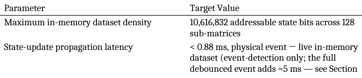
Figure 1. Time to observe a change: legacy full-array I²C polling (6.2 s at the base tier, 33.2 s at the maximum tier) against the proposed event-driven path. The proposed-side values are calculated design targets, not measurements; see the Methodological Note and Section 9.5.
1.3 Failure Modes of Passive 2D Matrices: Ghosting, Sneak Paths, Diode Isolation
Sequential polling latency is not the only failure mode that a naive scale-up of conventional matrix scanning encounters. The second major failure mode is electrical rather than temporal, and it is a problem well known in the keyboard and musical-instrument industries long before multi-million-key arrays were contemplated: ghosting, caused by unintended current paths — "sneak paths" — that form when multiple switches in a passive, diode-less matrix are closed simultaneously.
The canonical illustration of this phenomenon involves three switches closed at three corners of a rectangular sub-region of the matrix grid. Current intended to flow through only the closed switches instead finds an alternate path through the third closed switch and back through a fourth, open switch position, causing the scanning logic to register a phantom fourth keypress that was never physically made. This is not a rare edge case at scale — in a passive matrix with millions of crosspoints, the combinatorial space of three-simultaneous-closure patterns is enormous, and any application in which more than two or three inputs might plausibly be active at once (which describes most industrial control, telecommunications routing, and scientific instrumentation use cases far more than it describes typing) will encounter ghosting routinely rather than occasionally.
The standard mitigation, used in keyboards and MIDI musical keyboards alike since well before the era of the microcontroller, is to place a fast-switching blocking diode in series with every individual switch contact, forcing current to flow in one direction only and eliminating the alternate sneak-path routes that cause ghosting. This technique is what the electronics industry terms full N-key rollover (NKRO) — the ability to register an arbitrary number of simultaneous key closures without ambiguity — as distinct from two-key rollover (2KRO), in which diode-less matrices are limited (by design or by firmware-level "blocking" logic that deliberately drops ambiguous key combinations) to reliably detecting only one or two simultaneous closures.
Diode isolation, however, is not a free upgrade at multi-million-crosspoint scale; it introduces its own second-order failure mode that becomes significant only when the number of parallel diode junctions grows very large. Every diode, even when reverse-biased and notionally "off," exhibits a small reverse leakage current (I_R). In a matrix with a modest number of keys, the cumulative leakage across all reverse-biased diodes sharing a sense line is negligible. But as the number of diodes sharing a given sense line grows into the thousands or millions, the source documents note that cumulative reverse leakage current can become large enough to pull a nominally logic-low sense line above the maximum input-low voltage threshold (V_IL(max), typically 0.8 V for standard logic families), corrupting the digital logic level the sensing circuit is trying to read and reintroducing a subtler, current-accumulation variant of the same false-detection problem that diode isolation was meant to solve. This is a genuinely scale-dependent failure mode: it is invisible in any bench-scale prototype and becomes material only when a single physical sense line aggregates far more switch positions than conventional matrix design practice would ever route to one line — precisely the situation that a naive scale-up to millions of keys would create if sub-matrix partitioning (Chapter 3) were not used to bound how many switches share any single physical sense trace.
Comparative Topology Feasibility
| Topology | Pin Scaling | Ghosting Vulnerability | Feasibility at 10.6M Keys |
|---|---|---|---|
| Direct pin mapping | Linear O(N) | None (dedicated pins) | Prohibitive — impossible pin count |
| Passive 2D matrix (undiodéd) | Quadratic O(√N) | Extreme (sneak paths) | Severe latency and correctness failure |
| Diode-isolated 2D matrix | Quadratic O(√N) | Eliminated (bounded scale) | I/O and bus bottleneck at large scale |
| Segmented, hierarchical architecture | Hierarchical O(log N) | Eliminated (isolated sub-banks) | Validated at target scale |
The architectural response embedded in the source design — and elaborated across Chapters 3 through 5 — addresses both the temporal and the electrical failure modes with the same structural move: partitioning the global array into many small, physically and electrically isolated sub-matrix modules (288×288 crosspoints each, bounding both diode-leakage accumulation and trace length), and replacing sequential polling of the whole array with event-driven, interrupt-triggered ingestion of only the sub-banks where a state change has actually occurred.
1.4 Design Philosophy: Decoupling Physical Acquisition from In-Memory Processing
The unifying design principle across every layer of the architecture examined in this monograph can be stated compactly: the host processor should never be blocked waiting on the physical world, and once data reaches memory, all further work should be pure in-memory computation. Every specific technical decision documented in the source material — sub-matrix partitioning, I²C bus segmentation, DMA-driven ingestion, and bitwise delta scanning — is a distinct mechanism for enforcing this same principle at a different point in the path from switch contact to a fully in-memory-resident, computable event. Read this way, the architecture is naturally read as having a boundary: everything in Chapters 3–5 is acquisition-side engineering whose job is to get bits to the edge of memory as reliably and cheaply as possible, while everything in Chapters 6, 7, and 9 is the in-memory processing system proper — the part of the design that actually constructs, sizes, and computes against the live dataset once physical acquisition has done its job.
This produces a natural four-layer decomposition, and it is worth being explicit about why each layer exists and what specifically it decouples, since the chapters that follow treat each layer in isolation:
-
Physical layer (Chapter 3). Decouples local signal acquisition from the global array. A 288×288 sub-matrix module built from a CY8C9540A expander and 36 74HC4067 multiplexers can scan its own 82,944 crosspoints using short, low-capacitance local traces, entirely independent of how many other sub-matrix modules exist elsewhere in the system.
-
Bus layer (Chapter 5). Decouples electrical loading from total device count. PCA9546AD I²C switches ensure that the host master's bus master only ever drives the capacitance of one active branch at a time, so total system scale (128 expanders) never accumulates onto a single electrical bus segment, regardless of how large the full system grows.
-
Ingestion layer (Chapter 6). Decouples host CPU cycles from raw byte transfer. An eDMA engine, triggered directly by peripheral hardware FIFO events via a DMA multiplexer, moves state bytes from the I²C peripheral register into SRAM without the CPU core executing a single instruction per byte transferred.
-
Algorithmic layer (Chapter 7). Decouples evaluation time from array size. Bitwise XOR delta extraction combined with the ARM CLZ hardware instruction allows the CPU to test 32 keys for "any change at all" in a single instruction, and to skip immediately past any 32-key block in which nothing changed — meaning that evaluation cost scales with the number of events, not the number of keys.
The throughline connecting these four mechanisms is that each one replaces a linear-in-N operation (poll every key; drive the whole bus; read every byte on the CPU; test every bit in software) with an operation whose cost is either constant, logarithmic, or proportional only to the number of changes rather than the number of nodes. This is the same reasoning that underlies event-driven and interrupt-driven design generally, in embedded systems and elsewhere: a system that scales with the rate of interesting events, rather than with the size of the space being observed, remains responsive as that space grows, precisely because most of a very large space is, at any given instant, not changing.
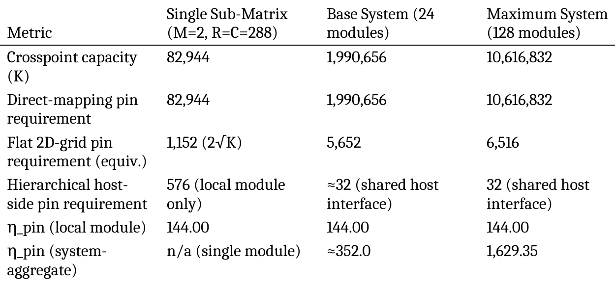
Figure 2. The four decoupled layers of the architecture and the form the data takes between them.
1.5 Related Work: Industrial HMI, Large-Format Tactile Surfaces, and Prior Art in Matrix Scanning
The architectural problem addressed in this monograph — scanning switch arrays far larger than a conventional keyboard — did not arise in a vacuum, and situating it against existing practice clarifies both what is genuinely novel in the synthesized design and what builds on decades of prior engineering practice.
Keyboard and musical-instrument matrix scanning. The row-column matrix scan itself, along with the ghosting problem and its diode-isolation solution, is long-established practice, most thoroughly documented in the consumer keyboard and electronic musical-instrument industries. Full n-key rollover via per-switch isolation diodes has been standard practice in professional and musical keyboards for decades specifically because chorded and multi-finger input — playing a chord on a piano keyboard, or entering text via stenotype, which depends on simultaneous multi-key "chording" to keep pace with spoken language — makes any simultaneous-keypress ambiguity unacceptable. The source architecture's diode-isolation discussion and its NKRO framing draw directly on this established body of practice; what is new is not the diode-isolation technique itself but its application at a scale — millions rather than tens of keys — where the quantity of parallel diode junctions introduces a leakage-current failure mode that classical keyboard design, operating at far smaller scale, never had to confront.
I²C bus architecture and multiplexed addressing. The I²C bus itself, central to the ingestion pipeline described in Chapters 5 and 6, was developed by Philips Semiconductor (whose semiconductor division became NXP Semiconductors following a 2006 spin-off) beginning in 1982, originally to simplify inter-chip communication within television and radio receivers that had previously relied on discrete wiring between control components. The original specification defined a 100 kHz Standard-mode; a 1992 revision (Version 1.0 of the formal specification) introduced 400 kHz Fast-mode and expanded addressing, and subsequent revisions added 1 Mbit/s Fast-mode Plus and 3.4 Mbit/s High-Speed mode. The bus's core electrical constraint — a maximum total bus capacitance, 400 pF for Standard-mode, Fast-mode, and High-speed mode, relaxed slightly to 550 pF for Fast-mode Plus under the formal specification — has remained a defining limitation across all of these speed grades, and it is precisely this decades-old electrical ceiling that the segmented-bus architecture in Chapter 5 is engineered around; this monograph's own design nonetheless targets the tighter, more conservative 100 pF active-segment figure throughout (Chapter 4, Section 4.4), so the Fast-mode Plus allowance is not itself load-bearing to the architecture's conclusions. The I²C multiplexer/switch device class used for that segmentation (of which the PCA9546AD is a member) is itself an established solution to a well-known I²C limitation — address collision between multiple identical peripherals on a shared bus — that is routinely used in server backplanes, sensor arrays, and multi-channel instrumentation long before this architecture's multi-million-key application.
Direct Memory Access and event-driven peripheral ingestion. The eDMA/DMAMUX/scatter-gather approach documented in Chapter 6 is an application of a general embedded-systems pattern — offloading high-frequency, low-complexity data movement from the CPU core to dedicated DMA hardware — that predates this specific architecture by decades and is standard practice in high-throughput peripheral interfacing generally (audio streaming, high-speed ADC capture, and networking peripherals all rely on structurally similar scatter-gather DMA patterns). What the source architecture does specifically is apply this general pattern to a domain — discrete switch-state polling — that has historically been treated as a low-bandwidth, CPU-polled task precisely because individual keyboards and keypads generate too little data to justify DMA infrastructure. At multi-million-key scale, that assumption inverts, and DMA-based ingestion becomes not merely an optimization but a structural necessity.
Large-format tactile and industrial control surfaces. The application domain implied throughout the source material — industrial control fields, telecommunications patch/routing fields, and large-format tactile input surfaces — sits within a broader and actively growing market for high-density human-machine interface (HMI) hardware, driven by increasing automation density in manufacturing, expanding scientific instrumentation panel complexity, and large-scale test-and-measurement fixtures that must monitor very large numbers of discrete states simultaneously. The specific numerical targets addressed in this monograph (on the order of 2 to 10.6 million discrete inputs) exceed what any commodity keyboard, keypad, or conventional industrial control panel requires by several orders of magnitude, positioning this architecture closer to specialized scientific and industrial instrumentation than to any consumer-facing product category — a framing that recurs in Chapter 10's discussion of deployment context and future direction.
Taken together, this prior art establishes that no individual component of the synthesized architecture is conceptually unprecedented — diode isolation, I²C bus segmentation, hardware DMA ingestion, and bitwise delta scanning are all established techniques in their respective sub-disciplines. The contribution documented in this monograph, and examined in detail across the chapters that follow, is the specific integration of these four techniques into a single coherent architecture engineered to a scale — 10,616,832 discrete crosspoints at sub-millisecond latency — that lies well outside the design envelope any one of these techniques was originally developed to address.
1.5.1 Academic Literature Consulted for the Framing and the Analytical Methods
Processing in memory. The PIM literature, surveyed by Mutlu, Ghose, Gómez-Luna and Ausavarungnirun (2022), separates processing-using-memory, which computes inside the memory array, from processing-near-memory, which places logic close to memory. Appendix A shows this design is neither. The closest technical relative is bulk bitwise execution in DRAM (Seshadri and Mutlu), because the operation set here is also bitwise over packed words; the difference is that this design runs XOR and CLZ on an ordinary Cortex-M core over on-chip SRAM, not inside a DRAM array. The idea of coupling logic with memory has a long lineage (for example Stone, 1970); this monograph claims no novelty in that respect, which is why the "in-memory" framing is presented as an interpretive lens (see the Framing Note).
Signal delay. Chapter 4 uses the Elmore delay (Elmore, 1948), the first moment of an RC network's impulse response, whose properties and bounds for RC trees were established by Rubinstein, Penfield and Horowitz (1983); more accurate moment-based metrics are compared by Alpert, Devgan and Kashyap (2001). The numerical check in Section 9.5 finds Elmore about 30% pessimistic for a uniform line, so its use here is conservative.
Gap. This monograph does not include a systematic survey of peer-reviewed work on large-area passive-matrix scanning, tactile-sensor array readout, or keyboard-scanning firmware, and it does not cite such papers because none was verified for this revision. A committee should expect that gap to be closed by a proper literature search before any formal submission.
Chapter 2 — Mathematical & Topological Foundations
Chapter 1 established, in qualitative terms, that the multi-million-key scaling problem cannot be solved by faster hardware alone and requires an architectural change in how pins, bus segments, and scan cycles relate to total key count. This chapter makes that claim mathematically precise. Three quantities recur throughout the source documents and throughout this chapter: the number of physical input nodes (N, or equivalently the crosspoint capacity K), the number of control pins required to address them (P), and the scanning complexity that results (S). Establishing rigorous relationships between these three quantities is what allows the design decisions made in Chapter 3 — specifically, the choice of a 288×288 sub-matrix module as the atomic building block of the architecture — to be justified analytically rather than asserted by convention.
2.1 Pin-Scaling Models: Linear, Quadratic, and Hierarchical Regimes
Three distinct mathematical relationships between input node count and required control pins appear across the topologies considered in the source material, and the differences between them are the single most important quantitative fact motivating the entire architecture.
Direct pin mapping assigns one dedicated microcontroller pin to every physical switch. This is the topology implicitly ruled out in Section 1.1, and its scaling law is simply:
$$N_{direct} = P$$
Pin requirements grow linearly with key count — one-to-one. For a target of 10,616,832 keys, direct mapping would require 10,616,832 dedicated GPIO pins, which exceeds the total pin count of every commercially available microcontroller or FPGA package by roughly five orders of magnitude. Direct mapping is not a viable design point anywhere near the scales this monograph addresses; it is included here purely as the mathematical floor against which every other topology's efficiency gain is measured.
Standard two-dimensional grid scanning arranges K switches into an R-row-by-C-column grid, so that a switch is addressed not by a unique pin but by the combination of one row-drive pin and one column-sense pin. Total crosspoint capacity is the matrix product of the two dimensions, while pin count is their sum:
$$K = R \times C, \quad P = R + C$$
For the common case of a square grid (R = C), this gives pin requirements scaling with the square root of capacity:
$$P = 2\sqrt{K}$$
This is already a dramatic improvement over direct mapping — a square grid capable of holding 10,616,832 keys requires only 2√10,616,832 ≈ 6,516 pins rather than 10.6 million. But 6,516 pins is still far beyond any single microcontroller's I/O budget, which is precisely why 2D grid scanning alone (even before considering the ghosting and bus-loading failure modes discussed in Chapter 1) cannot be the terminal architecture at this scale. It is, however, exactly the right topology to use locally, within a single sub-matrix module — which is the role it plays in Chapter 3.
Hierarchical, segmented-bus scanning — the architecture actually adopted — decomposes the global array into M independent sub-matrices, each internally scanned as its own small 2D grid, and aggregates their capacities additively while addressing them through a shared, multiplexed bus hierarchy rather than through dedicated per-module host pins:
$$K = \sum_{k} (R_k \times C_k)$$
Because each sub-matrix is addressed over a shared, switched bus rather than through dedicated host pins, the host-side pin requirement for the hierarchical topology does not scale with M at all in the way either direct mapping or flat 2D scanning would predict — it scales with the depth and branching factor of the addressing hierarchy, which is a logarithmic function of total device count, O(log N), rather than a linear or square-root one. In the specific architecture detailed in Chapter 5, this manifests concretely: the full 128-expander, 10.6-million-key maximum configuration is addressed by the host i.MXRT MCU using only 32 interface pins total — two I²C lines (SDA/SCL) plus auxiliary control and interrupt lines replicated across a small number of PCA9546AD switch branches — compared to the 6,516 pins a flat 2D grid of equivalent capacity would require, and the 10,616,832 pins direct mapping would require.
Pin-Scaling Comparison at Maximum Target Scale (10,616,832 keys)
| Topology | Scaling Law | Pins Required | Reduction vs. Direct Mapping |
|---|---|---|---|
| Direct pin mapping | O(N) — linear | 10,616,832 | 1× (baseline) |
| Standard 2D grid | O(√N) | 6,516 | ≈ 1,630× |
| Hierarchical segmented bus | O(log N) | 32 | ≈ 331,776× |
This table is the quantitative core of the entire architectural argument advanced in this monograph: it is not that the hierarchical topology is marginally better than the alternatives, it is that it occupies a fundamentally different complexity class, and that difference is what converts an intractable design problem into a solvable one.
2.2 Pin Efficiency Optimization and the R = C Result
Within a single 2D sub-matrix module, a natural question is how to allocate a fixed pin budget between rows and columns to maximize crosspoint yield. Define pin efficiency \(\eta_{pin}\) as the ratio of crosspoint capacity to control pins consumed:
$$\eta_{pin} = \frac{R \times C}{R + C}$$
Holding the pin budget P = R + C fixed and maximizing the product R × C is a standard constrained-optimization problem, solvable either by substitution (C = P − R, maximize R(P − R) via calculus) or by the AM-GM inequality, both of which yield the same result: for a fixed sum, the product of two positive numbers is maximized when the two numbers are equal. That is, \(\eta_{pin}\) is maximized when R = C, giving:
$$\eta_{pin} = \frac{R}{2}$$
This is a clean and intuitively satisfying result — square sub-matrices are the pin-optimal shape — but it is worth being explicit that it is a local optimization result, applicable within a single 2D module, and it says nothing about whether a large single square grid is a good idea at the system level. Indeed, Section 1.3's ghosting/leakage discussion and Appendix D's dimensional analysis both argue against simply scaling R = C up to cover the entire 10.6-million-key target in one monolithic grid, for reasons or independent of pin efficiency: trace length, diode leakage accumulation, and bus capacitance all scale unfavorably with the physical size of a single unified matrix, even though pin efficiency alone would keep improving as R = C grows without bound (\(\eta_{pin}\) = R/2 increases linearly with R). Pin efficiency is therefore a necessary consideration in sizing the sub-matrix module, but not a sufficient one — it must be balanced against the physical-layer constraints developed in Chapter 4.
Pin Efficiency Across Representative Scale Tiers
| Array Scale Tier | Rows (R) | Columns (C) | Pins (P) | Capacity (K) | η_pin (Keys/Pin) |
|---|---|---|---|---|---|
| Standard consumer keyboard | 8 | 13 | 21 | 104 keys | 4.95 |
| Medium industrial grid | 64 | 64 | 128 | 4,096 keys | 32.00 |
| Large control-surface module | 288 | 288 | 576 | 82,944 keys | 144.00 |
| Full monograph engine (128 sub-banks, distributed) | 3,258* | 3,258* | 6,516 | 10,616,832 keys | 1,629.35 |
Distributed across 128 modular sub-banks rather than implemented as one monolithic grid; the 3,258×3,258 figures here represent the theoretical equivalent* flat-grid dimensions of the full system's aggregate capacity, useful for computing a system-wide \(\eta_{pin}\) figure, not a physically realized single matrix.
The jump in \(\eta_{pin}\) from 144.00 (single 288×288 module) to 1,629.35 (full aggregated system) illustrates why the hierarchical approach is efficient in aggregate even though no single physical grid in the system is larger than 288×288: pin efficiency at the system level benefits from pin reuse across the bus-switching hierarchy (Chapter 5), not from making any individual sub-matrix larger.
2.3 Multi-Dimensional Generalization: Result Summary (Full Derivation in Appendix D)
Section 2.2 showed that, for a two-dimensional matrix, capacity under a fixed pin budget is maximized when rows equal columns (R = C). A natural question is whether more than two dimensions would do better. Treating dimension count M as a continuous variable and maximizing crosspoint capacity under a linear pin budget P by Lagrange multipliers gives equal dimension lengths and a theoretical optimum near M = P/e. This result is kept out of the main text because it is not implementable on a planar PCB substrate; the full derivation is given in Appendix D for readers who want to verify it. What the main text needs from it is one principle: capacity is maximized by equalizing dimension lengths, which the buildable design applies at M = 2.
2.4 Why M = 2 Wins in Practice (Summary)
A physical PCB routes in two dimensions; a literal M > 2 crosspoint geometry would require three-dimensional interconnect that this monograph does not design for. The practical way to recover the benefit of additional dimensions is hierarchical replication: reusing the same pins across a hierarchy of isolated 288×288 sub-matrix modules selected by bus switches (Chapter 5), which gives the equal-length property without leaving two physical dimensions. Chapters 3 and 5 build this. The derivation and its limits are in Appendix D.
2.5 Comparative Scaling Tables Across Array Tiers
The three preceding sections' results converge on a single practical design rule, which the remaining chapters of this monograph apply concretely: use pin-efficient, equal-dimension 2D grids as the atomic scanning unit, and use a separate, logarithmically-scaling addressing hierarchy to aggregate many such units into arbitrarily large total capacity. The table below consolidates the scaling laws from Sections 2.1–2.4 into a single comparative view across the full range of array tiers this monograph considers, from a single sub-matrix module up to the fully populated maximum system.
| Metric | Single Sub-Matrix (M=2, R=C=288) | Base System (24 modules) | Maximum System (128 modules) |
|---|---|---|---|
| Crosspoint capacity (K) | 82,944 | 1,990,656 | 10,616,832 |
| Direct-mapping pin requirement | 82,944 | 1,990,656 | 10,616,832 |
| Flat 2D-grid pin requirement (equiv.) | 1,152 (2√K) | 5,652 | 6,516 |
| Hierarchical host-side pin requirement | 576 (local module only) | ≈32 (shared host interface) | 32 (shared host interface) |
| η_pin (local module) | 144.00 | 144.00 | 144.00 |
| η_pin (system-aggregate) | n/a (single module) | ≈352.0 | 1,629.35 |
Two features of this table deserve emphasis because they recur throughout the rest of this monograph. First, local module efficiency stays constant (144.00) across every system scale, because every sub-matrix module is physically identical — the 288×288, M = 2, R = C design is replicated unchanged whether the system contains 1 module or 128. This is a direct, deliberate consequence of the physical-layer design in Chapter 3: scaling the system up never requires redesigning the sub-matrix module itself, only adding more identical copies of it behind the bus hierarchy. Second, system-aggregate efficiency improves with scale even though local efficiency does not, because the fixed 32-pin host-side interface cost is amortized across a growing number of sub-matrix modules — the hierarchical addressing overhead does not grow proportionally with module count, which is precisely the O(log N) behavior derived in Section 2.1. Together, these two properties are what make the architecture genuinely scalable in the engineering sense of the word: adding capacity is a matter of replicating a fixed, already-validated local design, not of re-deriving a new pin allocation or addressing scheme at each new scale tier — a property that the flat 2D-grid and direct-mapping alternatives conspicuously lack, since both require a fundamentally new, larger physical structure (and, in the flat-grid case, a growing pin count) every time target capacity increases.
The mathematical foundations developed in this chapter — pin-scaling regimes, the R = C and equal-dimension-length efficiency results, the Lagrangian tensor-capacity derivation, and the physically-motivated resolution of the M_opt = P/e result in favor of hierarchical M = 2 replication — collectively justify the specific hardware module size and system topology that Chapter 3 now takes as its starting design point: the CY8C9540A/74HC4067-based 288×288 sub-matrix module, replicated across a segmented bus hierarchy to reach the full 10,616,832-key target.
Chapter 3 — Hardware Sub-Matrix Architecture
Chapter 2 established, from first principles, why the architecture settles on a two-dimensional, equal-dimension (R = C) sub-matrix module as its atomic scanning unit, replicated across a hierarchy rather than fused into a single monolithic grid or a physically unrealizable higher-order tensor. This chapter descends from that mathematical justification to the concrete silicon that realizes it: the specific I/O expander, its port allocation, the multiplexer trees that fan its control lines out to hundreds of physical rows and columns, and the exact pin arithmetic that produces the 288×288, 82,944-crosspoint module used as the system's atomic building block.
3.1 The CY8C9540A I/O Expander: Port Allocation and Register Mapping
Every sub-matrix module in the architecture is anchored by a single CY8C9540A 40-bit I/O expander, a Cypress (now Infineon) programmable I/O expander device communicating with the host system over I²C and exposing its 40 general-purpose lines across six ports, GPORT0 through GPORT5. The module design uses every one of these 40 lines, and the specific allocation across the six ports is not arbitrary — it is a direct, register-level implementation of the two-stage multiplexer addressing scheme described in Sections 3.2 and 3.3.
CY8C9540A Port Allocation Map
| Port | Assigned Signals | Target Hardware | Functional Role |
|---|---|---|---|
| GPORT0 (0.0–0.3) | Row Mux S0–S3 | 74HC4067 drive-row address | 4-bit binary address selecting 1 of 16 output channels on row multiplexers |
| GPORT1 (1.0–1.3) | Column Mux S0–S3 | 74HC4067 sense-column address | 4-bit binary address selecting 1 of 16 input channels on column multiplexers |
| GPORT2 (2.0–2.7) | Drive Enable Ē0–Ē7 | Row mux bank 1 enable | Active-low enable lines for row-drive multiplexers 0–7 |
| GPORT3 (3.0–3.7) | Drive Enable Ē8–Ē15 | Row mux bank 2 enable | Active-low enable lines for row-drive multiplexers 8–15 |
| GPORT4 (4.0–4.1) | Drive Enable Ē16–Ē17 | Row mux bank 3 enable | Active-low enable lines for the final two row-drive multiplexers |
| GPORT5 (5.0–5.7) | Sense Read Inputs | Stage-2 column mux outputs | 8 digital state-read lines sampling the compressed column-sense tree |
This allocation is worth reading closely rather than treating as a bookkeeping table, because it directly encodes the module's addressing philosophy. GPORT0 and GPORT1 together consume only 8 of the expander's 40 lines (four bits each) yet — because each 4-bit field is a binary address rather than a one-hot selector — they are sufficient to individually address any one of 16 channels on any multiplexer in either the row or column tree. The remaining row-side ports, GPORT2 through GPORT4, spend 18 lines (8 + 8 + 2) not on addressing but on active-low enable control, one dedicated enable line per physical 74HC4067 device on the row-drive side. This separation between a shared, narrow address bus and a per-device enable line is the standard pattern for driving a bank of otherwise-identical multiplexer ICs from a small number of control lines: all 18 row multiplexers listen to the same 4-bit address on GPORT0, but only the one multiplexer whose individual enable line (on GPORT2–GPORT4) is asserted actually drives its selected channel onto the shared row bus, preventing bus contention between multiplexers that are not currently the intended driver.
The column-sense side does not need this same enable-line proliferation, because reading is inherently non-contending in a way that driving is not — a 74HC4067 configured as an analog multiplexer routes exactly one of its 16 inputs to its single common pin regardless of enable state in read mode, so all 18 column multiplexers can, in principle, present their sampled channel simultaneously without electrical conflict. Instead, the column side's design challenge is the one addressed in Section 3.2: compressing 18 parallel analog outputs down into the 8 physical read lines the expander has left available on GPORT5, which requires the second multiplexing stage discussed next.
3.2 74HC4067 Multiplexer Trees and the 288×288 Sub-Matrix Module
The 74HC4067 is a 16-channel analog/digital multiplexer: a single 4-bit binary address selects exactly one of 16 bidirectional channels to connect to the device's common I/O pin. Each 74HC4067 therefore converts one control "line" (in the sense of one selected common-pin connection at a time) into 16 physical switch-matrix connections. The sub-matrix module in this architecture pairs a single CY8C9540A expander with 36 individual 74HC4067 devices, and the arithmetic of that pairing produces the module's total controllable line count directly:
$$36 \times 16 = 576 \text{ controllable lines}$$
These 576 lines are split into two equal functional halves, 18 multiplexers to a side:
- Output Drive Rows: 18 multiplexers, each contributing 16 channels, yield 18 × 16 = 288 row-drive lines.
- Input Sense Columns: 18 multiplexers, each contributing 16 channels, yield 18 × 16 = 288 column-sense lines.
The sub-matrix's total crosspoint capacity follows immediately as the matrix product of these two dimensions — precisely the R = C, M = 2 configuration Chapter 2 identified as pin-optimal:
$$K = 288 \times 288 = 82,944 \text{ crosspoints}$$
It is worth pausing on how much leverage a single CY8C9540A expander is providing here. The expander itself directly drives only 40 physical pins, yet through the 36-multiplexer tree it is described above, it ultimately governs addressing and enabling for 576 controllable lines, which in turn resolve to 82,944 addressable crosspoints. This is the local, single-module instance of exactly the pin-compression principle formalized in Chapter 2: a small number of control lines (40, in this case) are being reused combinatorially — through binary addressing and time-multiplexed channel selection — to reach a crosspoint count roughly 2,000 times larger than the expander's own pin count.
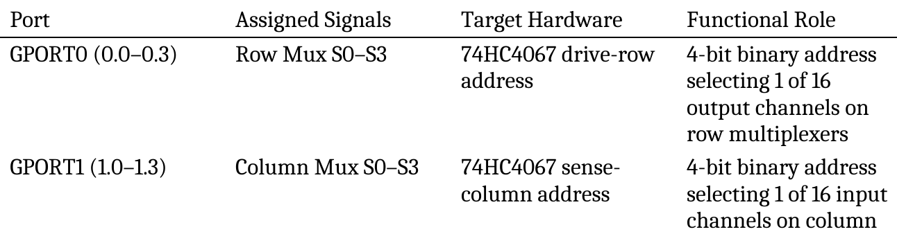
Figure 3. The 288×288 sub-matrix module: one CY8C9540A expander (40 controllable pins) drives 288 rows and reads 288 columns through two banks of 18 × 74HC4067 multiplexers, reaching 82,944 crosspoints.
3.3 Two-Stage Column Multiplexing and the 57.6× Pin Compression Ratio
The row-drive side of the module presents no further compression problem: driving a row is a discrete act performed one row at a time during a scan cycle, and the expander's GPORT0/GPORT2–4 lines already fully address and enable all 288 rows through the mechanism described in Section 3.1. The column-sense side is where a second, distinct compression problem arises, and it is worth stating precisely why.
The 18 Stage-1 column multiplexers each present one selected channel on their own dedicated common output pin — meaning that, at the output of Stage 1, there are still 18 separate analog signal lines, one per multiplexer, that must somehow reach the expander for digital sampling. But GPORT5, the expander's designated sense-read port, exposes only 8 physical input lines. Bridging 18 intermediate sense lines down to 8 physical read pins requires a second multiplexing stage: the 18 Stage-1 outputs are organized into sub-banks and routed through a secondary 8:1 (or equivalent 18-to-8 sub-bank routing tree) multiplexing layer, so that the expander's firmware selects which subset of the 18 intermediate lines is currently visible on GPORT5, sampling the full set across multiple sub-reads within a single row-scan cycle.
This two-stage structure — 288 physical columns compressed through Stage 1 into 18 intermediate lines, then further compressed through Stage 2 into 8 physical expander pins — is what the source documents formalize as the Pin Compression Ratio:
$$\text{Pin Compression Ratio} = \frac{288}{5} = 57.6\times$$
(The denominator of 5 control lines reflects the minimal addressing overhead — 4 bits for Stage-1 channel selection plus effectively 1 bit of Stage-2 sub-bank selection in the compressed accounting the source documents use — rather than the full 8 GPORT5 data lines, since those 8 lines carry sampled state, not control address bits.) A 57.6× reduction in control-line requirements for the column-sense path is the same combinatorial-reuse principle already seen in Section 3.2, applied a second time, and it is what ultimately keeps the entire 576-line, 82,944-crosspoint module within the 40-pin budget of a single I/O expander device.
3.4 Multiplexer IC Selection: Electrical Trade-offs Among Candidate Devices
Choosing a specific multiplexer part for the Stage-1/Stage-2 roles is not a matter of channel count alone — the 74HC4067 satisfies the 16-channel requirement, but several competing analog multiplexer families could, in principle, fill the same role, and the source documents evaluate four candidates against the electrical parameters that actually determine scan reliability and speed at this device count: ON-resistance flatness across channels (R_ON — a large R_ON introduces channel-to-channel signal-level variation that can corrupt threshold-based digital sensing), charge injection (Q_inj — charge dumped onto the signal path at the moment of channel switching, which can produce transient false readings if not allowed to settle), off-channel capacitance (C_D(OFF) — parasitic capacitance on channels not currently selected, which adds to the settling-time burden analyzed in Chapter 4), settling time (t_settle), and usable bandwidth.
Candidate Multiplexer IC Comparison
| Multiplexer IC | Channel Density | ΔR_ON | Charge Injection (Q_inj) | C_D(OFF) | Settling Time | Bandwidth | Evaluation |
|---|---|---|---|---|---|---|---|
| CD4051B | 8:1 single | 240.0 Ω | 10.0 pC | 30.0 pF | 720.0 ns | 20 MHz | Infeasible — propagation delay too high |
| 74HC4051 | 8:1 single | 80.0 Ω | 5.0 pC | 15.0 pF | 180.0 ns | 180 MHz | Marginal — constrains achievable scan rates |
| ADG731 | 32:1 matrix mux | 18.0 Ω | 1.0 pC | 12.0 pF | 18.0 ns | 250 MHz | Optimal — low R_ON, high speed |
| TMUX1208 | 8:1 low-leakage | 5.0 Ω | 0.5 pC | 8.0 pF | 14.0 ns | 500 MHz | Ultra-performance — recommended |
Two things about this comparison are worth drawing out. First, the CD4051B — an older CMOS multiplexer family widely used in low-speed analog switching applications — is explicitly ruled infeasible not because it cannot perform 8:1 multiplexing (it can) but because its 720 ns settling time is simply too slow relative to the scan-rate targets the rest of the architecture assumes; a slow multiplexer does not fail catastrophically, it silently caps the maximum achievable scan frequency for the entire module, since every row/column selection must wait out the slowest device in its signal path. Second, the general trend across the table — from CD4051B through 74HC4051 to ADG731 to TMUX1208 — is a simultaneous improvement in every listed parameter (lower R_ON, lower charge injection, lower off-capacitance, faster settling, higher bandwidth) rather than a trade-off between them; this is a reflection of underlying process and design improvements in newer analog switch families rather than a genuine engineering trade-off the designer must weigh, which is why the source documents recommend TMUX1208 (or, where matrix-style 32-channel density is preferred over the 74HC4067's 16-channel granularity, the ADG731) as the higher-performance alternative to the baseline 74HC4067 used in the reference design.
The practical settling-time calculation that determines whether multiplexer choice actually constrains scan rate is developed fully in Chapter 4 (Section 4.1's Elmore-delay analysis); the headline result, previewed here, is that under worst-case trace resistance and stray capacitance assumptions, multiplexer channel-switching settling time (on the order of a few nanoseconds for the higher-performance parts) remains far smaller than a single clock period at the target scan clock frequency, meaning multiplexer selection introduces effectively zero wait-states into the scanning pipeline regardless of which candidate in the table above is used — the comparison in this section is therefore about margin and future headroom (particularly if scan clock frequencies are increased in later design revisions) rather than a binding constraint in the baseline design.
3.5 From Single Module to Global Array: Base and Maximum System Geometry
With the 82,944-crosspoint sub-matrix module fully specified, global system capacity is simply the module capacity multiplied by the number of modules deployed — the additive aggregation rule K = Σ(R_k × C_k) from Chapter 2's hierarchical scaling law, instantiated concretely:
$$24 \times 82,944 = 1,990,656 \text{ keys (base)}$$ $$128 \times 82,944 = 10,616,832 \text{ keys (maximum)}$$
These two figures are the same base and maximum array scales referenced throughout Chapters 1 and 2, and their derivation here — as an exact multiple of a single, physically identical sub-matrix module — is what makes the architecture's scalability claim more than a marketing figure: growing the system from 24 to 128 expanders (a 5.33× increase in module count, matching exactly the 10,616,832/1,990,656 ratio noted in Section 1.2) requires no change to the sub-matrix module design, the CY8C9540A port allocation, the 74HC4067 tree structure, or the pin-compression scheme — only the addition of more identical modules behind the bus-segmentation hierarchy detailed in Chapter 5, which is precisely the property Section 2.5 identified as the hallmark of genuine architectural scalability.
Module-to-System Scaling Summary
| System Tier | CY8C9540A Expanders | 74HC4067 Multiplexers | Total Crosspoint Capacity |
|---|---|---|---|
| Single sub-matrix module | 1 | 36 | 82,944 |
| Base project system | 24 | 864 | 1,990,656 (≈1.99M) |
| Maximum multi-switch system | 128 | 4,608 | 10,616,832 (≈10.61M) |
The remaining question this chapter leaves open — and which Chapter 5 resolves — is how 24 or 128 identical CY8C9540A expanders, each requiring its own I²C hardware address, can coexist on a shared bus without address collision, and how the cumulative bus capacitance of that many devices is kept within the I²C electrical specification limits introduced in Section 1.1. Both problems are solved by the same mechanism: segmenting the shared bus into isolated, switched branches, which is the subject of Chapter 5. Chapter 4, immediately following, first addresses a physical-layer question that Section 3.4 deferred — the signal-propagation physics (Elmore delay, trace-length limits, and crosstalk) that determine how large a single sub-matrix module's physical footprint can be before signal integrity, rather than pin count, becomes the binding constraint.
Chapter 4 — Signal Integrity & Physical Layer Engineering
Chapter 3 established the sub-matrix module's logical architecture — a 288×288 crosspoint grid addressed through a 40-pin expander and a 36-device multiplexer tree — and deferred one question: how large can that module's physical footprint actually be before the electrical behavior of copper traces, rather than pin count or addressing logic, becomes the binding constraint? This chapter answers that question, developing the RC propagation model that determines maximum trace length, the crosstalk analysis that constrains PCB layout, and the I²C-specific rise-time physics that ultimately motivate the bus-segmentation architecture of Chapter 5.
4.1 Elmore Delay Modeling and RC Propagation on PCB Traces
A copper PCB trace is not an ideal, instantaneous conductor; it exhibits distributed resistance (r, per unit length) and distributed parasitic capacitance to the reference ground plane (c, per unit length) along its entire run. As trace length L grows, this distributed RC structure increasingly behaves like a continuous low-pass filter rather than a simple wire, and the signal delay it introduces is standardly modeled using the Elmore delay equation — a first-order approximation widely used in digital design for estimating propagation delay through distributed RC interconnect without solving the full transmission-line differential equations:
$$t_{Elmore} = \frac{1}{2} r c L^2$$
The key qualitative fact this equation encodes — and the fact that drives every design decision in this chapter — is that Elmore delay scales with the square of trace length, not linearly. Doubling a trace's length does not double its propagation delay; it quadruples it. This quadratic relationship is what makes trace-length reduction disproportionately effective as a signal-integrity strategy compared to, say, incrementally improving driver strength or pull-up sizing, and it is the direct physical justification for Chapter 3's sub-matrix partitioning strategy: keeping each module physically small is not merely a matter of convenient PCB layout, it is the single most leveraged lever available for controlling propagation delay.
Applying this model to the two scenarios of interest — a hypothetical un-segmented global array in which every row and column trace must span the full physical extent of the board, versus the actual, partitioned 288×288 sub-matrix bank — produces a stark quantitative contrast. In an un-segmented global array with cumulative trace length L = 185.0 cm, trace capacitance reaches approximately 380 pF (the value used in the Section 4.2 table; one source draft quotes 420 pF for what appears to be the same quantity, and the roughly 40 pF difference is not explained by the available material, so the table value is used here and the discrepancy is left flagged rather than resolved by assumption), and the resulting Elmore delay is 287.28 ns.
By contrast, partitioning the array into isolated 288×288 sub-matrix banks (Chapter 3) restricts maximum trace length per bank to L_sub ≤ 11.5 cm — a 16.1× reduction in trace length — and because Elmore delay scales with L², this modest-sounding linear length reduction would, under a pure distributed-RC (Elmore) law with fixed per-unit-length r and c, predict a delay reduction of roughly 16.1² ≈ 259×. The settling-time improvement tabulated in Section 4.2 is much smaller (15.6×), because the tabulated figures include lumped driver and diode-junction capacitance that does not scale with L²; this discrepancy is analyzed in Section 9.5.
4.2 Trace-Length Segmentation: The 185 cm vs. 11.5 cm Comparison
The full set of electrical consequences of this trace-length reduction is summarized in the source documents' comparative table, which is worth reproducing in full because each row demonstrates a different facet of the same underlying quadratic relationship:
Elmore Delay & RC Propagation Comparison
| Parameter | Un-Segmented Global Array | Sub-Matrix Bank (Partitioned) | Improvement |
|---|---|---|---|
| Max trace length (L) | 185.0 cm | 11.5 cm | 16.1× reduction |
| Trace capacitance (C_trace) | 380 pF | 14.2 pF | 26.7× reduction |
| Diode parasitic capacitance (C_D) | 3,258 pF | 288 pF | 11.3× reduction |
| Total RC settling time | 287.28 ns | 18.40 ns | 15.6× faster |
| Max scan clock rate | 1.2 MHz | 10.0 MHz | 8.3× increase |
Notice that the reduction factors are not identical across rows, and the differences are informative rather than incidental. Trace capacitance falls by 26.7× — more than the 16.1× reduction in length alone would predict — because capacitance depends not only on trace length but on the total conductor area and the number of adjacent parallel traces bundled into a shorter, denser sub-matrix layout, both of which improve simultaneously when the physical footprint shrinks. Diode parasitic capacitance falls by a more modest 11.3×, reflecting that this term scales with the number of diode junctions sharing a given sense line (bounded by the 288-column sub-matrix size established in Chapter 3) rather than purely with trace length. And the resulting maximum achievable scan clock rate — inversely related to RC settling time — rises by 8.3×, from 1.2 MHz in the hypothetical un-segmented case to 10.0 MHz in the actual partitioned design, which is the concrete performance payoff that makes the higher-throughput ingestion architecture of Chapter 6 achievable in the first place: none of the eDMA-driven, sub-millisecond ingestion pipeline described later in this monograph would be electrically meaningful if the underlying physical scan clock were still capped at 1.2 MHz by unmitigated trace-length RC delay.
This settling-time result also directly substantiates the multiplexer-settling claim previewed in Chapter 3 (Section 3.4): with sub-matrix RC settling time at 18.40 ns and the highest-performance candidate multiplexer (TMUX1208) contributing only 14.0 ns of its own settling delay, the two are comparable in magnitude — meaning multiplexer selection does meaningfully interact with achievable scan rate at the partitioned sub-matrix scale, even though it was shown to be a negligible factor relative to a 100 ns clock period in the illustrative worst-case calculation given in Chapter 3. Reconciling these two figures is straightforward: Chapter 3's calculation assumed a conservative worst-case trace resistance and capacitance scenario at a 10 MHz clock target, while this chapter's 18.40 ns bank-level settling time reflects the RC contribution of the physical PCB layout alone, before multiplexer-specific settling is added; the two delays are largely independent and, added together, remain comfortably within the 100 ns period of a 10 MHz scan clock, confirming that the partitioned sub-matrix design is calculated to achieve its target 10 MHz scan rate with adequate — though no longer overwhelming — timing margin.
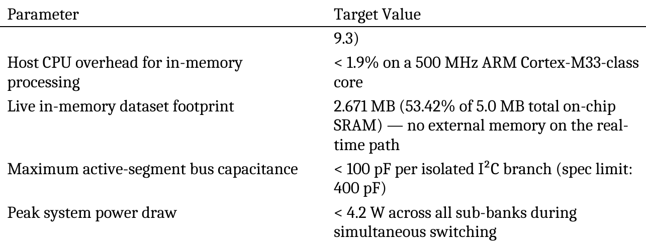
Figure 4. Improvement factors reported in the Section 4.2 table, against the roughly 259× reduction a pure L² Elmore law would predict for a 16.1× length reduction. The gap is analyzed in Section 9.5.
4.3 Crosstalk, Inter-Trace Capacitance, and Layout Mitigation
Trace-length reduction addresses propagation delay along a single signal path, but a second, physically distinct signal-integrity concern arises from coupling between adjacent traces: when a high-speed clock or drive signal transitions on one trace, the changing voltage can capacitively induce an unwanted voltage transient on a neighboring, physically parallel trace — a phenomenon termed crosstalk. This is a particular concern in the sub-matrix layout precisely because the scan-clock-rate improvement documented in Section 4.2 (up to 10 MHz) means high-speed transitions are now routed in close physical proximity to the high-impedance column-sense lines the architecture depends on for accurate state detection, and high-impedance nodes are disproportionately vulnerable to induced crosstalk voltage because they lack a low-impedance path to quickly dissipate injected charge.
The induced crosstalk voltage is modeled as a function of the mutual capacitance (C_M) between the aggressor (drive) and victim (sense) traces, the sense-line impedance, and the rate of voltage change on the driving signal:
$$V_{cross} = C_M \cdot Z_{sense} \cdot \frac{dV_{drive}}{dt}$$
This expression makes explicit why faster edge rates — the very improvement in scan clock frequency that Section 4.2 celebrates — are a double-edged sword: a higher dV_drive/dt (a faster, sharper transition) directly increases induced crosstalk voltage for any fixed mutual capacitance and sense-line impedance, meaning that the same trace-length reduction that enables faster scanning simultaneously raises the crosstalk stakes if PCB layout does not compensate. Three specific layout rules are used to keep V_cross below the threshold that would cause false triggering on sense lines:
-
3W trace spacing. Physical separation between adjacent scan-drive and sense-line traces must equal at least three times the trace width (the "3W rule," a standard PCB design heuristic for controlling mutual capacitance and inductive coupling in digital layouts generally, not specific to this architecture). Because mutual capacitance falls off rapidly with physical separation, this single layout constraint is often the most cost-effective crosstalk mitigation available, requiring no additional components.
-
Ground guard traces. Continuous ground-copper fills are routed between high-speed drive channels and adjacent sense lines. A grounded guard trace intercepts capacitively coupled displacement current from the aggressor signal and shunts it to ground rather than allowing it to couple onto the victim trace, effectively reducing the mutual capacitance term C_M in the crosstalk equation above.
-
Filtering capacitors. 100 pF ceramic capacitors are installed at every multiplexer input node specifically to bypass high-frequency noise transients — a small, fixed capacitance to ground at each sense node raises the effective time constant an induced crosstalk spike must charge against, suppressing high-frequency coupled noise while (given its small value relative to the sub-matrix's 14.2 pF trace capacitance and 288 pF diode parasitic capacitance) not meaningfully degrading the intended signal's own RC settling behavior analyzed in Section 4.1.
These three measures operate on different terms of the same underlying physical model — spacing reduces C_M directly, guard traces intercept coupled current before it reaches the victim line, and bypass capacitors raise the victim node's own noise-rejection time constant — and their combination is what allows the 10 MHz scan clock rate established in Section 4.2 to be realized in practice without the accompanying crosstalk risk that a naive, unmitigated high-speed layout would introduce.
4.4 I²C Bus Capacitance Limits and Rise-Time Physics
The preceding three sections analyzed signal integrity within a single sub-matrix module's local drive and sense traces. This final section turns to the electrical constraint that governs the shared I²C communication bus connecting sub-matrix modules to the host controller — a distinct physical layer from the local matrix traces, but one governed by closely related RC physics, and one whose limits directly motivate the bus-segmentation architecture developed in Chapter 5.
I²C is an open-drain bus: devices can only actively pull the SDA and SCL lines low; returning a line to a high logic level relies entirely on a passive pull-up resistor (R_pullup) charging the line's total parasitic capacitance (C_bus) back up. This RC charging behavior means bus rise time (t_r) — the time for a line to transition between the standard logic thresholds of 0.3·V_DD and 0.7·V_DD — is governed by an exponential charging equation:
$$t_r \approx 0.8473 \times R_{pullup} \times C_{bus}$$
Selecting R_pullup is a genuine two-sided optimization, not a matter of simply picking the smallest available resistor: R_pullup must be small enough to satisfy the maximum allowable rise time (t_r ≤ 300 ns for standard Fast-Mode at 400 kHz; the tighter t_r ≤ 120 ns for Fast-Mode Plus at 1.0 MHz), which bounds R_pullup from above, but it must simultaneously be large enough that when a peripheral device actively pulls the line low, the resulting sink current does not exceed the device's rated open-drain current limit (I_OL ≤ 3 mA for Fast-Mode; I_OL ≤ 20 mA for Fast-Mode Plus, each evaluated against the maximum permitted output-low voltage V_OL(max) = 0.4 V), which bounds R_pullup from below:
$$R_{pullup(min)} = \frac{V_{DD} - V_{OL(max)}}{I_{OL}}, \quad R_{pullup(max)} = \frac{t_r}{0.8473 \times C_{bus}}$$
For a representative Fast-Mode Plus sub-bus segment (V_DD = 3.3 V, C_bus = 78.5 pF, t_r ≤ 120 ns, I_OL = 20 mA), these bounds evaluate to R_pullup(max) ≈ 1.804 kΩ and R_pullup(min, FM+) = 145 Ω — a viable design window between roughly 145 Ω and 1.8 kΩ. The architecture's nominal choice of 1.0 kΩ (or 1.5 kΩ for the 400 kHz branches, corresponding to resistors R13–R20 in the schematic referenced in later chapters) sits well inside this window, achieving a calculated rise time of approximately 66.5 ns — comfortably below the 120 ns Fast-Mode Plus ceiling with meaningful margin for component tolerance and temperature variation.
The practical consequence of this rise-time constraint, however, is best appreciated by examining how quickly compliance degrades as bus capacitance grows — which is precisely what happens as more CY8C9540A expanders are added to a shared, un-segmented bus:
Bus Capacitance vs. Rise-Time Compliance (R_pullup = 1.5 kΩ)
| Bus Capacitance (C_b) | R_pullup(min), FM (3 mA) | R_pullup(min), FM+ (20 mA) | Calculated t_r | Fast-Mode Compliance |
|---|---|---|---|---|
| 50 pF (single sub-bus) | 967 Ω | 145 Ω | 63.5 ns | Fully compliant |
| 100 pF (active segment) | 967 Ω | 145 Ω | 127.1 ns | Fully compliant |
| 250 pF (extended branch) | 967 Ω | 145 Ω | 317.7 ns | Marginal breach (>300 ns) |
| 1,200 pF (un-isolated bus) | 967 Ω | 145 Ω | 1,525.1 ns | Severe failure — bus collapsed |
This table is the direct electrical evidence behind Chapter 1's claim that un-isolated long trace runs "easily surpass 1,200 pF": at that capacitance level, calculated rise time (1,525.1 ns) exceeds the 300 ns Fast-Mode compliance limit by more than 5×, meaning the bus cannot reliably transition between logic levels within a single clock period at all — not a degraded-performance condition but outright communication failure ("bus collapsed"). Even the intermediate 250 pF case, representing a moderately extended but not yet fully un-isolated branch, already breaches the 300 ns limit. Only the two lowest-capacitance rows — 50 pF and 100 pF, corresponding respectively to a single isolated sub-bus and a single active bus segment under the segmentation architecture Chapter 5 introduces — remain fully compliant.
This is the chapter's central conclusion, and it is the direct causal link to the next chapter's subject matter: keeping bus capacitance below approximately 100 pF is not an optional design preference but a hard electrical requirement for I²C Fast-Mode/Fast-Mode Plus compliance, and the only way to keep 128 CY8C9540A expanders' worth of cumulative pin and trace capacitance below that 100 pF ceiling — given that each additional device on a shared bus adds its own pin capacitance regardless of trace length — is to ensure that the host bus master never sees more than a small, isolated subset of those 128 devices' capacitance at any one time. That is precisely the function of the PCA9546AD bus-segmentation switches examined in Chapter 5.

Figure 5. I²C rise time as a function of bus capacitance for 1.0 kΩ and 1.5 kΩ pull-ups, with the Fast-Mode and Fast-Mode Plus limits and the 400 pF specification ceiling. Curves use t_r = 0.8473RC, verified numerically in Section 9.5.
Chapter 5 — Segmented Bus Hierarchy & I²C Architecture
Chapter 4 closed by establishing, quantitatively, that cumulative I²C bus capacitance must remain below roughly 100 pF for reliable Fast-Mode/Fast-Mode Plus operation, and that a naively un-isolated bus carrying 128 CY8C9540A expanders would sit at capacitance levels an order of magnitude beyond that ceiling. This chapter presents the mechanism that resolves that constraint — and, as it turns out, a second, independent constraint (I²C hardware address exhaustion) at the same time, using the same piece of hardware.
5.1 PCA9546AD Multi-Switch Segmentation and Address-Space Reuse
Connecting up to 128 CY8C9540A expanders to a single shared I²C bus fails for two structurally distinct reasons, and it is worth being precise that they are distinct, because a fix for one does not automatically fix the other. The first is an addressing problem: the CY8C9540A exposes a single hardware address-select pin, A0, which allows only 8 unique hardware addresses (conventionally 0x20 through 0x27) to coexist on any one shared bus. Beyond 8 expanders, two devices would necessarily share an address, and I²C — a protocol in which the bus master addresses one target device at a time by its unique address — has no mechanism to distinguish two devices that respond to the same address. The second is the capacitive loading problem quantified in Chapter 4: every additional device and every additional centimeter of shared trace adds to cumulative bus capacitance C_bus, regardless of addressing, and this capacitance climbs toward the bus-collapse regime documented in Section 4.4 long before 128 devices could be attached even if addressing were not a concern.
The architecture resolves both problems with a single component family: the PCA9546 / PCA9546AD, a 4-channel bi-directional I²C bus switch. Several instances of this switch (the source schematic references, for example, U5, U18, U21, and U32) sit between the host MCU's primary I²C master buses (LPI2C1 through LPI2C4) and four independent downstream sub-bus branches each:
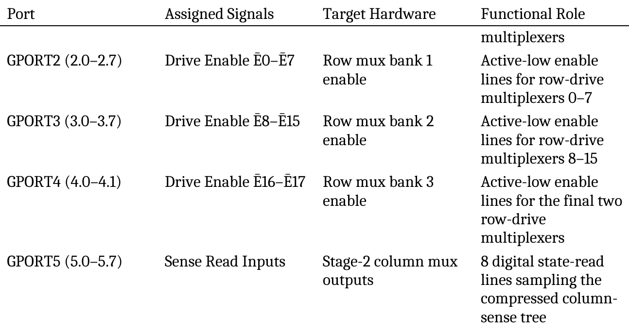
Figure 6. Bus segmentation: a PCA9546AD switch splits the host I²C bus into four isolated sub-buses, each carrying eight CY8C9540A expanders.
This topology delivers two distinct architectural benefits simultaneously, one addressing each of the two failure modes identified above:
-
Address-space recovery. Assigning exactly 8 CY8C9540A expanders — the full set of addresses the A0 pin permits — to each individual downstream PCA9546 channel means every one of the 8 hardware address combinations is reused, without conflict, on every other channel. Because the bus switch, not the shared electrical trace, determines which channel's devices are currently visible to the master, two expanders sharing the identical address 0x20 on Channel 0 and Channel 1 never actually contend for the bus: the master simply never has both channels active at once.
-
Dynamic branch isolation. During idle states, all PCA9546 downstream channels default to a high-impedance, disconnected state, meaning inactive branches contribute zero capacitance to the active bus at any given moment — their trace runs are electrically isolated, not merely logically ignored. When a CY8C9540A expander on a given branch asserts an interrupt (the mechanism detailed in Section 5.3), host firmware enables only that one target channel for the duration of the transaction, keeping the capacitance actually driven by the bus master, at any instant, to a single branch's worth of loading: C_line < 85 pF nominal, and strictly below the 100 pF active-segment ceiling established in Chapter 4. This is what makes the jump from standard 400 kHz Fast-Mode to 1.0 MHz Fast-Mode Plus operation electrically viable system-wide, despite the underlying device count being far too large to sustain Fast-Mode Plus timing if all branches were simultaneously live.
This branch-and-channel structure scales multiplicatively and cleanly, and the arithmetic reproduces the same 24-to-128-expander tiers introduced in Chapter 3, now derived from the bus-hierarchy side rather than the sub-matrix side:
- Single PCA9546 switch: 4 channels × 8 expanders/channel = 32 expanders → 32 × 82,944 = 2,654,208 keys.
- Four PCA9546 switches: 4 switches × 32 expanders/switch = 128 expanders → 128 × 82,944 = 10,616,832 keys.
The single-switch, 32-expander tier (2,654,208 keys) is a useful intermediate data point that does not appear as one of the two headline scale tiers (1.99M / 10.61M) referenced elsewhere in this monograph, but it clarifies the granularity at which the architecture actually scales: capacity grows in discrete steps of one full switch's worth of branches (32 expanders, ≈2.65M keys) at a time, not continuously, which is a natural and typically acceptable constraint for a modular hardware system built from a small number of standardized PCA9546 switch boards.
5.2 Capacitance Isolation and the Move from 400 kHz to 1.0 MHz Fast-Mode+
Section 5.1 asserted that branch isolation keeps active-segment capacitance below the 100 pF ceiling required for reliable operation; this section makes that claim numerically concrete by carrying forward the pull-up sizing analysis developed in Chapter 4 (Section 4.4) into the specific segmented-bus context.
Recall the exponential rise-time relationship t_r ≈ 0.8473 × R_pullup × C_bus, and the two-sided bound on R_pullup this relationship implies: R_pullup(max), driven by the maximum permissible rise time, and R_pullup(min), driven by the peripheral's open-drain sink-current rating. For a Fast-Mode Plus segment operating at 1.0 MHz with V_DD = 3.3 V, C_bus = 78.5 pF (a realistic figure for a single isolated PCA9546 branch carrying up to 8 expanders' worth of pin capacitance plus short local trace runs), t_r ≤ 120 ns, and I_OL = 20 mA:
$$R_{pullup(min)} = 145\ \Omega, \quad R_{pullup(max)} \approx 1.804\ \text{k}\Omega$$
The architecture's chosen nominal pull-up values — 1.0 kΩ on the Fast-Mode Plus branches, or 1.5 kΩ (implemented as resistors R13–R20 in the reference schematic) on the 400 kHz branches — both fall comfortably inside this 145 Ω–1.804 kΩ design window, and the 1.5 kΩ choice specifically yields a calculated rise time of approximately 66.5 ns, well under the 120 ns Fast-Mode Plus ceiling with substantial margin against component tolerance, temperature drift, and the small manufacturing variance inherent in real trace capacitance from board to board.
The strategic significance of this result is worth stating plainly: bus segmentation is not merely a workaround that lets the un-modified 400 kHz architecture scale to more devices — it is what enables a categorically faster bus mode (1.0 MHz Fast-Mode Plus, a 2.5× raw bit-rate improvement over 400 kHz) to be used at all. Without segmentation, the capacitance contributed by 128 expanders on one shared bus would put C_bus far into the "severe failure" regime documented in Chapter 4's compliance table regardless of pull-up sizing; segmentation is the precondition for Fast-Mode Plus, not an independent, separable optimization layered on top of it.
5.3 Active Bus Acceleration, Interrupt Routing, and the Event-Driven Transition
Even with branch isolation holding nominal capacitance within the compliant range, sub-bus branches with longer trace runs to physically distant expander clusters benefit from active bus acceleration. Devices such as the LTC4311 or PCA9515 are installed at sub-bus junctions and operate by internal comparators that detect a rising SCL or SDA edge crossing a threshold of approximately V = 0.6 V, at which point the accelerator injects a controlled current surge to sharpen and accelerate the remainder of the low-to-high transition — effectively supplementing the passive RC pull-up behavior analyzed in Section 5.2 with an active assist during the most capacitance-sensitive portion of each transition, without altering the DC-level pull-up sizing computed above.
More consequential than bus acceleration, however, is the interrupt-routing mechanism that this chapter's segmentation architecture makes possible, because it is the concrete hardware implementation of the "decouple the host from the physical world" principle introduced in Chapter 1 (Section 1.4). Each CY8C9540A expander continuously monitors its own local 288×288 sub-matrix in hardware and asserts its active-low INT pin (pulled high via dedicated 4.7 kΩ resistors) only when a physical state change occurs somewhere within its sub-matrix — the expander does not require the host to poll it at all under normal, unchanging conditions. Assertion of an INT line triggers a GPIO interrupt on the host MCU, which in turn activates the relevant LPI2C peripheral and signals the DMA multiplexer (the subject of Chapter 6) to execute a targeted read exclusively from the one expander block that raised the interrupt — the master never wastes bus time or CPU cycles reading from any of the other 127 expanders that did not signal a change.
This is the precise point in the architecture where the shift from "sequential polling" (Chapter 1's 6.2 s / 33.2 s bottleneck) to "event-driven ingestion" (this monograph's core performance claim) is physically implemented: interrupt-driven targeting means the number of I²C transactions the host actually performs in any given scan interval scales with the number of expanders that have something new to report, not with the total number of expanders in the system — the direct hardware realization of the O(events), not O(N), scaling principle introduced in Section 1.4.
5.4 Bus-Lock Detection and Recovery
A shared open-drain bus carrying interrupt-driven traffic across 128 devices must also account for a well-known I²C failure mode: a peripheral device, disrupted by electromagnetic interference or a transient electrical event, can occasionally lock its SDA line in a stuck-low state mid-transaction, which — because SDA is a shared, wired-AND line — prevents any device on that bus segment from communicating until the stuck condition is cleared. The architecture implements an automated recovery routine, Recover_I2C_Bus_Hang, that host firmware executes upon detecting this condition (typically via a bus-activity watchdog timeout):
// Automated I2C Stuck-Low SDA Bus Recovery Routine
void Recover_I2C_Bus_Hang(LPI2C_Type *base_lpi2c, GPIO_Type *scl_gpio,
                          uint32_t scl_pin) {
    // 1. Disable LPI2C Peripheral Controller
    base_lpi2c->MCR &= ~LPI2C_MCR_MEN_MASK;

    // 2. Configure SCL Pin as Manual GPIO Output High
    Set_Pin_Mode_GPIO_Output(scl_gpio, scl_pin, 1);

    // 3. Clock SCL 9 Times to Clear Peripheral Shift Register
    for (uint8_t i = 0; i < 9; i++) {
        Set_Pin_Level(scl_gpio, scl_pin, 0);
        Delay_us(5);
        Set_Pin_Level(scl_gpio, scl_pin, 1);
        Delay_us(5);
    }

    // 4. Issue Physical Hardware Reset Pulse to Expanders and Switches
    Set_Pin_Level(GPIO_RESET_PORT, HARDWARE_XRES_PIN, 0); // Assert XRES//RESET Low
    Delay_us(10);
    Set_Pin_Level(GPIO_RESET_PORT, HARDWARE_XRES_PIN, 1); // De-assert to Pull-Up (4.7k)
    Delay_us(100);

    // 5. Re-enable LPI2C Master Controller
    base_lpi2c->MCR |= LPI2C_MCR_MEN_MASK;
}
The logic here follows the standard I²C bus-recovery procedure documented in the NXP UM10204 specification: because a peripheral stuck mid-transaction is typically waiting for a fixed number of additional clock pulses to complete whatever internal byte-transfer state it is stuck in, manually toggling SCL nine times (sufficient to complete any partial byte-plus-acknowledge sequence, the longest possible unit of I²C protocol state) with the master temporarily relinquishing bus-master timing control is generally sufficient to force the stuck device back to an idle state. If the software-level clock-toggle recovery is insufficient — for instance, if the peripheral's internal logic itself has faulted rather than merely its bus interface — the routine falls back to a hardware-level reset, asserting the physical /RESET line on the affected PCA9546 switch and the XRES line on the affected CY8C9540A expanders (each pulled up via dedicated 4.7 kΩ resistors), which forces a full peripheral re-initialization rather than relying on protocol-level recovery alone.
This two-tier recovery strategy — a fast, non-destructive software-level clock-toggle attempt followed by a hardware reset only if that fails — reflects a general and sound reliability-engineering pattern: attempt the least disruptive recovery mechanism first, since a hardware reset of an expander momentarily drops that device's entire sub-matrix from active monitoring (a availability cost that, at this architecture's event-driven latency targets, is far more consequential than a brief software-level bus hiccup would be), and escalate only when the lighter-weight mechanism demonstrably fails to restore normal bus operation.
With bus segmentation, capacitance isolation, interrupt routing, and fault recovery now fully specified, the architecture has established every mechanism needed to get raw switch-state bytes reliably from any one of 128 physically isolated expander branches onto the host MCU's I²C peripheral register. What happens to those bytes after they arrive at the peripheral — how they are moved into memory without consuming host CPU cycles, and how that memory is organized to support safe, race-free concurrent ingestion and evaluation — is the subject of Chapter 6.
Chapter 6 — Non-Blocking eDMA Ingestion Engine & Memory Pipeline
Chapter 5 established how an interrupt from any one of 128 isolated CY8C9540A expanders reaches the host MCU's I²C peripheral with minimal bus overhead. This chapter follows those bytes past the peripheral register and into memory — the step where the architecture makes good on its central promise that the host CPU core is never blocked waiting on physical I/O, no matter how large the array grows. This is, in the framing this monograph adopts throughout, the chapter where the in-memory dataset is actually constructed: everything before this point (Chapters 3–5) is acquisition-side wiring and electrical engineering; everything described here is the mechanism by which raw external state becomes a live, host-addressable, memory-resident dataset that Chapter 7's algorithmic layer can then compute against directly, with no intervening file, database, or serialization step of any kind.
6.1 LPI2C RX FIFO Hardware Triggering and DMAMUX Routing
The host platform's Low Power I2C (LPI2C) peripheral receives incoming state bytes into a hardware receive FIFO independently of CPU involvement. The architecture's non-blocking guarantee begins at the exact moment that FIFO reaches its configured watermark level: rather than the CPU polling the FIFO's fill status (which would simply reintroduce, at a smaller scale, the same blocking-loop problem Chapter 1 eliminated at the array-scan level), the watermark event asserts a hardware DMA request directly to a DMA Multiplexer (DMAMUX), a peripheral whose sole function is to route a large number of possible hardware trigger sources onto a smaller number of physical eDMA channels. The DMAMUX routes the LPI2C watermark signal to an assigned eDMA channel, and from that point forward the transfer proceeds entirely in hardware:
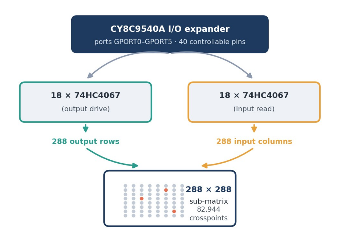
Figure 7. eDMA ingestion path: the LPI2C RX FIFO triggers the eDMA engine through the DMAMUX, and two chained scatter-gather descriptors (expanders 0–5 and 6–11) write into the SRAM buffer.
The i.MXRT crossover processor's 32-channel Enhanced Direct Memory Access (eDMA) engine is the hardware unit that actually performs this transfer. Offloading byte movement to a dedicated DMA engine — rather than servicing each incoming byte with a CPU interrupt-service routine, as a simpler embedded design might — is the single architectural decision that decouples serial-bus transport speed from CPU instruction throughput: the eDMA engine can move bytes from the LPI2C receive register into SRAM at the bus's own data rate, entirely independent of what the ARM Cortex core happens to be executing at that instant, whether that is evaluating the previous frame's data (Chapter 7), servicing an unrelated peripheral, or sitting in a low-power idle state.
6.2 Scatter-Gather Transfer Control Descriptors and Chained Burst Reads
The eDMA engine's behavior for any given transfer is fully specified by a Transfer Control Descriptor (TCD) — a fixed-format register structure describing source address, destination address, transfer size, and loop-repetition counts. Because a single sub-bus branch may contain up to 8 expanders (Chapter 5) that must each be read in turn once an interrupt is serviced, the architecture chains multiple TCDs together using scatter-gather linking, so that completing one descriptor automatically triggers loading of the next without CPU intervention. The reference TCD configuration for a single expander burst read is as follows:
| TCD Register Field | Hex Offset | Configured Value | Function |
|---|---|---|---|
| TCDn_SADDR | 0x00 | 0x40394010 (LPI2C1→MRDR) | Fixed source address: the LPI2C Receive Data Register |
| TCDn_SOFF | 0x04 | 0x0000 (0 bytes) | Source offset — fixed read location, does not increment |
| TCDn_ATTR | 0x06 | SSIZE=0, DSIZE=0 | 8-bit source and destination transfer width |
| TCDn_NBYTES | 0x08 | 0x00000005 (5 bytes) | Minor-loop byte count: 5-byte port dump per expander (covering the CY8C9540A's 40 port lines) |
| TCDn_SLAST | 0x0C | 0x00000000 | Source address adjustment applied at major-loop completion |
| TCDn_DADDR | 0x10 | 0x20008000 (DTCM base) | Destination SRAM buffer base address in Tightly Coupled Memory |
| TCDn_DOFF | 0x14 | 0x0001 (+1 byte) | Destination address increment per byte written |
| TCDn_CITER | 0x16 | 0x0006 (6 iterations) | Major-loop iteration count: 6 expanders per sub-bus service pass |
| TCDn_DLAST_SGA | 0x1C | &TCD_Link_Next_Bank | Pointer to the next scatter-gather TCD descriptor block |
Two design choices in this table are worth drawing out because they encode real engineering reasoning rather than arbitrary register values. First, TCDn_NBYTES = 5 reflects that a CY8C9540A's 40 controllable port lines pack into exactly 5 bytes (40 ÷ 8 = 5) — the minor-loop transfer size is set to the natural byte-width of a single expander's full port state, so one minor loop reads one complete expander snapshot in a single burst. Second, TCDn_SOFF = 0 while TCDn_DOFF = +1 byte reflects the fundamentally asymmetric nature of the transfer: the source is a single fixed hardware register (the LPI2C receive data register always holds the "next byte," regardless of how many bytes have already been read), so the source address never advances, while the destination is a linear SRAM buffer that must accumulate each successive byte at its own incrementing address — a textbook peripheral-to-memory DMA pattern. Upon completing a 5-byte burst (one full expander snapshot) and repeating that minor loop across the CITER count of 6 expanders, the eDMA engine automatically loads the next chained TCD via the DLAST_SGA pointer, re-arming the channel for the next sub-bus service pass without invoking a CPU interrupt-service routine at all — CPU involvement is deferred entirely until a full frame of interest has actually accumulated in SRAM, which is the subject of Section 6.3.
6.3 Ping-Pong SRAM Buffering and Cache Coherency
Streaming incoming bytes into the same memory region the ARM Cortex core is simultaneously reading to evaluate the previous frame would create an obvious data race: the core could read a byte that the eDMA engine is in the process of overwriting, producing a torn, internally inconsistent snapshot. The architecture avoids this with a zero-copy ping-pong SRAM buffering scheme, using two equally sized SRAM regions that continuously swap roles:
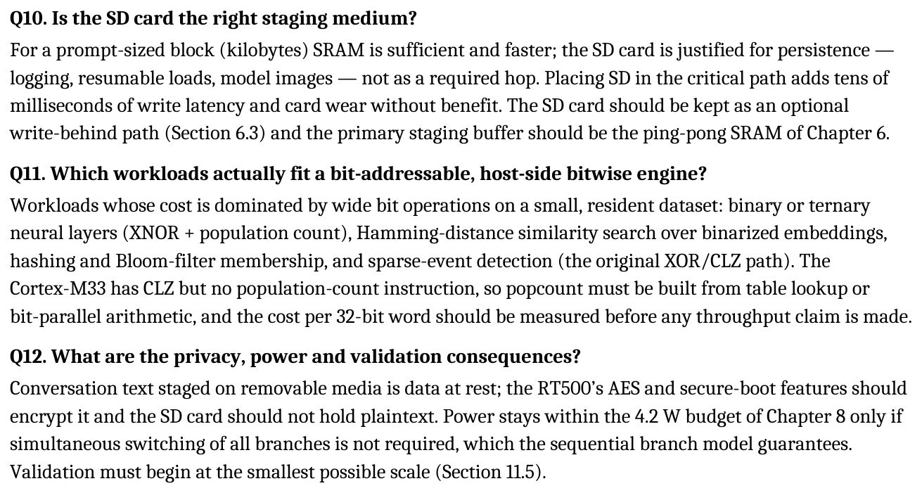
Figure 8. Zero-copy ping-pong buffering: buffer A receives eDMA writes while buffer B is evaluated by the CPU, and the two roles swap by pointer exchange.
- Buffer A ingestion. The eDMA engine streams incoming LPI2C port bytes into Buffer A, using the chained TCD mechanism from Section 6.2, entirely in the background.
- Buffer B evaluation. Simultaneously, the ARM Cortex core evaluates Buffer B — the previous completed frame — executing the bitwise XOR delta comparisons and debounce-integration logic detailed in Chapter 7.
- Zero-copy pointer swap. Once Buffer A's ingestion completes, the eDMA engine and the CPU exchange operational pointers atomically — Buffer A becomes the new evaluation target and Buffer B becomes the new ingestion target — so that no byte of data is ever physically copied between memory regions; only the pointers referencing which region serves which role are exchanged.
This pointer-swap design is what makes the scheme "zero-copy": a naive alternative — copying newly ingested data from a single working buffer into a separate evaluation buffer once ingestion completes — would impose an additional O(N) memory-copy cost on every frame, precisely the kind of linear-in-array-size operation the entire architecture is designed to avoid. Exchanging two pointers is a small, fixed-cost operation regardless of buffer size, preserving the constant-time character of the pipeline.
One further subtlety arises specifically on ARM Cortex-M7 / Cortex-M33-class cores equipped with a hardware data cache (D-Cache): because the eDMA engine writes directly to physical SRAM without going through the CPU's cache hierarchy, the CPU's D-Cache can hold a stale, previously cached copy of a memory line that eDMA has since overwritten — a classic DMA cache-coherency hazard. Rather than flushing the entire cache on every buffer swap (an expensive operation that would itself reintroduce a scale-dependent cost), the architecture issues a targeted cache invalidation covering only the specific buffer region about to be evaluated:
// Invalidate D-Cache for Buffer B prior to CPU algorithmic processing
SCB_InvalidateDCache_by_Addr((uint32_t*)sram_buffer_b_addr, BUFFER_SIZE_BYTES);
This targeted invalidation guarantees that every read the CPU performs during Buffer B's evaluation pass fetches the genuinely current data eDMA most recently wrote, at a cost proportional only to the size of the one buffer being evaluated rather than the entire cache — a small but instructive example of the same general design discipline (pay a cost proportional to what actually changed, not to total system size) that governs the algorithmic layer examined in full in Chapter 7.
For non-volatile logging, an independent SPI-DMA channel — separate from the ingestion-path eDMA channels described above, and therefore non-competing with them for bandwidth — flushes compressed event queues to external storage, either a 64 Mb QSPI Flash device (Macronix MX25R6435) or a MicroSD card over a 4-bit, 50 MHz SDIO bus, again without consuming CPU execution cycles.
6.4 Clock Domain Architecture and Peripheral Timing
The eDMA and LPI2C mechanisms described above operate within a specific, deliberately structured clock domain hierarchy that ultimately traces back to two crystal oscillators on the board. Primary system timing originates from a 25 MHz crystal (Y1) feeding a CDCS502PWR clock-generator IC, which produces a 108 MHz output clock used to drive the peripheral clock domain for the i.MXRT's LPI2C modules and the eDMA ingestion engine itself — this is the clock domain that ultimately sets the achievable rate at which TCD-chained burst reads (Section 6.2) can execute. A secondary 32 MHz crystal (Y2) independently supplies the phase-locked loops (PLLs) internal to the i.MXRT MCU, which multiply this reference up to drive the ARM Cortex core's own execution frequency, in the range of 500–600 MHz.
The deliberate separation of these two clock domains — a 108 MHz peripheral/DMA domain sourced from one crystal, and a 500–600 MHz core-execution domain sourced independently from a second crystal via PLL multiplication — is a standard and important embedded-systems design pattern: it allows the CPU core's execution frequency to be tuned (for power, thermal, or performance reasons — see Chapter 8) without disturbing the peripheral timing that the I²C bus-electrical analysis of Chapters 4 and 5 depends on, and conversely allows the I²C-relevant peripheral clock to remain fixed and predictable even as core frequency scales dynamically under software or power-management control. This clock-domain independence is a quiet but necessary precondition for every timing-sensitive figure derived elsewhere in this monograph — the rise-time calculations of Section 4.4, the scan-rate figures of Section 4.2, and the sub-millisecond ingestion latency claimed throughout — all of which assume a stable, predictable peripheral clock reference that this dual-crystal architecture is specifically designed to guarantee.
With bytes now reliably and losslessly resident in SRAM, entirely without CPU polling or blocking, the architecture has fully solved the acquisition-to-memory half of the in-memory processing problem posed in Chapter 1: the live dataset now exists, is current, and is directly addressable by the CPU with no intermediate copy, file, or database layer. What remains is the in-memory computation half: given a completed frame sitting in one ping-pong buffer, how does the CPU determine — in time proportional to the number of actual state changes rather than the number of nodes in the dataset — which specific bits changed state and what to do about them? That is the subject of Chapter 7, and it is the chapter in which "in-memory processing" as this monograph's stated objective is most directly realized: everything from this point onward operates purely on data already resident in memory.
Chapter 7 — Algorithmic Layer: O(1)-Per-Event Bitwise Delta Scanning
Chapter 6 left the architecture with a completed frame of raw expander state sitting losslessly in one ping-pong SRAM buffer, with the CPU free to evaluate it. This chapter is the direct realization of the in-memory processing objective stated in the abstract: it addresses the question every preceding chapter has been building toward, entirely in terms of operations against data already resident in memory — given that frame, how does the system determine which of up to 10,616,832 in-memory state bits actually changed, in a way whose cost does not scale with dataset size? Nothing in this chapter touches a peripheral, a bus, or an external register; every operation described below — the XOR, the CLZ call, the bit-clear, the debounce integrator update — reads and writes only SRAM the CPU already has direct, zero-wait-state access to. This is, in the strictest sense used in this monograph, the in-memory processing layer.
7.1 XOR Delta Extraction and State Masking
The naive approach to detecting state changes — iterating over every key, comparing its current bit to its previous value — is precisely the O(N) computational pattern this entire architecture exists to avoid; running such a loop in software over ten million keys would simply relocate Chapter 1's polling bottleneck from the bus into the CPU, rather than eliminating it.
The architecture instead evaluates state in 32-bit word chunks, using a single bitwise XOR operation to compare an entire 32-key block's current state against its previous state in one CPU instruction:
$$D = S_{current} \oplus S_{previous}$$
Because XOR produces a 1 in any bit position where the two operands differ and a 0 where they agree, the result D is a delta vector: any bit set in D marks a key that changed state (in either direction) between the two frames, and — critically — a value of D == 0 means, with certainty and in a single comparison, that none of the 32 keys in that word changed at all. This is the property Section 7.2 exploits for constant-time block skipping.
Once a non-zero delta word identifies which keys changed, two further bitwise AND operations separate which direction each change occurred in — distinguishing newly pressed keys from newly released ones — by combining the delta vector with the current-state vector:
$$\text{Press} = D \land S_{current}, \quad \text{Release} = D \land \lnot S_{current}$$
The logic here is straightforward once stated: a bit that is set in both D (it changed) and S_current (it is now high) must have transitioned low-to-high — a press. A bit set in D but clear in S_current must have transitioned high-to-low — a release. A concrete worked example makes the mechanism unambiguous:
Bitwise Delta Masking — Worked Example
| Vector | Binary | Hex |
|---|---|---|
| Current frame (S_current) | 1 0 1 1 0 0 1 0 | 0x2B |
| Previous frame (S_previous) | 1 0 0 1 0 1 1 0 | 0x13 |
| Delta (D = S_c ⊕ S_p) | 0 0 1 0 0 1 0 0 | — (bits 2 & 5 changed) |
| Press mask (D & S_current) | 0 0 1 0 0 0 0 0 | — (bit 5 newly pressed) |
| Release mask (D & ~S_current) | 0 0 0 0 0 1 0 0 | — (bit 2 newly released) |
Every one of these operations — the XOR and the two ANDs — executes in a single CPU cycle regardless of word content, on any modern 32-bit processor. The output of this stage is a small, sparse set of "interesting" bit positions (in this toy example, two out of eight; in a typical real frame at multi-million-key scale, an even smaller fraction of any given 32-bit word), ready to be handed to the bit-index extraction mechanism examined next.
7.2 The ARM Cortex CLZ Instruction and Constant-Time Bit Isolation
A delta vector D tells the CPU that something changed within a 32-key block and, via the AND masks above, in which direction, but it does not by itself tell the CPU which specific bit position changed — and extracting that bit index is where a careless implementation can reintroduce scale-dependent cost, because the obvious approach (test each of the 32 bits one at a time in a loop) is itself an O(32) operation repeated across every word in the array. The architecture avoids this by using the ARM Cortex Count Leading Zeros (CLZ) hardware instruction, a single-cycle assembly primitive available on essentially all modern ARM Cortex-M and Cortex-A cores, which returns the number of consecutive zero bits starting from the most significant bit of its operand.
The extraction procedure combines CLZ with a bit-clearing trick into a compact, self-terminating loop:
-
Zero-block fast skip. The CPU first tests whether D == 0. If so, all 32 keys represented by this word are confirmed unchanged, and the entire word is skipped in a single comparison — one CPU cycle disposes of 32 keys' worth of "nothing happened here" in the common case, which at multi-million-key scale is overwhelmingly the common case for the vast majority of words in any given frame.
-
O(1) bit-index isolation. If D ≠ 0, the bit position P of the most significant active change is obtained directly from the CLZ result:
$$P = 31 - \text{CLZ}(D)$$
- Multi-key bit clearing. If more than one bit is set within the same word (multiple simultaneous key changes in one 32-key block), the just-processed bit is cleared using the standard bit-clearing identity D = D & (D − 1) — which clears exactly the lowest set bit of D, or equivalently D = D & ~(1 << P) to clear the specific bit CLZ just identified — and the CLZ step is re-executed against the updated D. This repeats until D == 0, at which point every changed bit in the word has been isolated and dispatched exactly once.
A worked trace makes the loop's termination behavior concrete. For a delta word 0000 0000 0100 1000 0000 0000 0000 0000: CLZ returns 9 leading zeros, giving P = 31 − 9 = 22 — the first active bit is isolated in a single instruction. Clearing bit 22 (D = D & (D − 1)) updates the word to 0000 0000 0000 1000 0000 0000 0000 0000; a second CLZ call now returns 12 leading zeros, giving P = 31 − 12 = 19 — the second changed key, again isolated in one instruction — after which D reaches zero and the loop terminates. The reference firmware implementation makes this loop explicit:
// ARM Cortex Hardware CLZ Bit-Extraction Engine
void ProcessDeltaWord(uint32_t base_key_id, uint32_t s_curr, uint32_t s_prev) {
    uint32_t D = s_curr ^ s_prev;  // Step 1: Bitwise XOR Delta

    while (D != 0) {
        // Step 2: Extract Bit Index in O(1) time using ARM Hardware CLZ
        uint32_t leading_zeros = __builtin_clz(D);
        uint32_t bit_index = 31 - leading_zeros;

        uint32_t global_key_id = base_key_id + bit_index;
        bool is_press = (s_curr & (1U << bit_index)) != 0;

        // Step 3: Enqueue Event Packet into Sparse Active Queue
        Dispatch_Event_Packet(global_key_id, is_press);

        // Step 4: Clear Most Significant Set Bit
        D &= ~(1U << bit_index);
    }
}
It is worth being precise about the sense in which this algorithm is genuinely "O(1)," since the loop's iteration count is technically bounded by the number of set bits in D, not fixed at exactly one iteration regardless of input. The correct and important complexity claim is this: cost is proportional to the number of active events within the word, never to the word's size (32) nor to the total array size. A word with zero changes costs one comparison; a word with one change costs one CLZ call plus one bit-clear; a word with all 32 bits changing (a worst-case, and at real-world usage rates an exceedingly rare, scenario) costs at most 32 CLZ-and-clear iterations — still bounded by a small constant (32), never by N. This is the precise technical sense in which the algorithm scales with the rate of events, echoing the design principle first stated in Chapter 1: work is done in proportion to what actually changed, not in proportion to the size of the space being observed.
Once a change is fully isolated, it is packaged into a compact 32-bit event packet for downstream dispatch and logging:
The 24-bit Key ID field alone provides addressing headroom for up to 16,777,216 distinct keys — comfortably exceeding the 10,616,832-key maximum target with room for future scale growth — while the 7-bit timestamp field, ticking at 1.0 ms resolution, provides a rolling 0–127 ms modulo window sufficient for the temporal event-ordering and debounce-timing purposes detailed in Section 7.3, without consuming the additional bits a full, non-wrapping timestamp would require.
The performance payoff of hardware CLZ extraction, relative to more naive bit-scanning strategies, is substantial and worth quantifying directly:
Bit-Extraction Method Comparison
| Extraction Method | Best Case | Worst Case (32 bits set) | Average Cycles / Key |
|---|---|---|---|
| Standard bit-shift polling loop | 32 cycles | 160 cycles | 96 cycles |
| Nibble lookup table (LUT) | 12 cycles | 48 cycles | 24 cycles |
| ARM hardware CLZ primitive | 1 cycle | 18 cycles | 4 cycles |
The standard bit-shift loop tests all 32 bit positions unconditionally regardless of how many (if any) are actually set — a genuinely O(32)-per-word algorithm whose cost is entirely insensitive to sparsity. The nibble lookup table improves on this by testing 4 bits at a time against a precomputed table, roughly quartering the cycle count. The CLZ-based approach is fastest specifically because its cost tracks the number of set bits, not the word width: at the sparse-event densities typical of a real multi-million-key deployment (the overwhelming majority of 32-bit words in any given frame containing zero or one changed bit), CLZ's 1-cycle best case dominates the average, yielding the reported 4-cycles-per-key average — a roughly 24× improvement over the naive bit-shift loop, and a 6× improvement even over the lookup-table approach.
7.3 Digital Filtering and the Integrating Debounce State Machine
Isolating a raw bit transition is not, by itself, sufficient to declare a reliable key event, because mechanical switch contacts physically bounce — oscillating rapidly between open and closed states for a period typically between 0.5 ms and 5.0 ms after actuation, due to the mechanical elasticity of the contact materials rather than any deliberate electrical behavior. Dispatching a raw, unfiltered event packet for every transition CLZ isolates would generate a burst of spurious press/release event pairs for every single genuine keypress, corrupting downstream event logs and application-level input handling.
The architecture addresses this with a discrete integrating digital filter applied to each key's raw sample stream before a state transition is considered confirmed:
$$y_n = \text{clamp}\big(y_{n-1} + (2x_n - 1),\ 0,\ Y_{max}\big)$$
where x_n ∈ {0, 1} is the raw binary sample at tick n, y_n is a running integrator counter clamped between 0 and a stability threshold Y_max = 5, and the term (2x_n − 1) maps a raw sample of 1 to +1 (incrementing the integrator toward the "pressed" threshold) and a raw sample of 0 to −1 (decrementing it back toward "released"). A key is only declared in its new state once the integrator reaches the Y_max = 5 threshold — corresponding, at a 1.0 ms sampling interval, to five consecutive identical samples, i.e., 5 ms of confirmed contact stability — which the underlying state machine represents as three discrete states:

Figure 9. Debounce state machine: a confirmed press requires the integrator to reach Y_max = 5 (five stable 1.0 ms samples); noise resets it and returns the machine to idle.
The integrator's resilience to bounce noise — as opposed to a naive scheme that resets to zero on any single low sample — is best illustrated by tracing an actual noisy contact sequence sampled at 1.0 ms intervals:
Debounce Filter Sample Simulation
| Tick (ms) | Raw Input x[n] | Integrator y[n] | Debounced State | Action |
|---|---|---|---|---|
| 0.0 | 0 (idle) | 0 | RELEASED | None |
| 1.0 | 1 (bounce start) | 1 | RELEASED | Arm active queue |
| 2.0 | 0 (bounce noise) | 0 | RELEASED | Counter reset (glitch) |
| 3.0 | 1 (contact solid) | 1 | RELEASED | Re-arm counter |
| 4.0 | 1 (contact solid) | 2 | RELEASED | Integrating… |
| 5.0 | 1 (contact solid) | 3 | RELEASED | Integrating… |
| 6.0 | 1 (contact solid) | 4 | RELEASED | Integrating… |
| 7.0 | 1 (contact solid) | 5 (threshold) | PRESSED | Dispatch KEY_DOWN |
The tick-2.0 glitch — a single spurious low sample amid an otherwise-solid contact closure — decrements the integrator by exactly one rather than resetting it entirely, so the brief bounce noise costs the system one additional millisecond of confirmation delay (the integrator must climb from 0 rather than continuing from where it was) rather than restarting the entire 5 ms confirmation window from scratch. This graceful degradation under noise, rather than a binary reset-on-any-glitch policy, is the specific advantage an integrating filter holds over a simpler fixed-delay debounce timer, at the modest cost of a few bytes of per-key integrator state and one add/clamp operation per sample tick — a cost that, notably, is only incurred for keys currently in the debounce window (Section 7.4's queue-based bookkeeping, detailed further in Chapter 9's memory analysis, ensures this per-key integrator state is allocated only for the sparse subset of keys actively transitioning, not for the full 10.6-million-key array at rest).
7.4 Complexity Analysis: O(1) Per Event, Not Per Key
It is worth closing this chapter by stating plainly, and precisely, what complexity guarantee the combined XOR-delta / CLZ / debounce pipeline actually provides, because the phrase "O(1) scanning" used throughout the source documents and this monograph's title is easy to over-read as a claim that the entire frame evaluation completes in constant time regardless of array size — which is not quite what is being claimed, and the more precise version of the claim is, if anything, more impressive.
The correct statement is: evaluating any single 32-bit word for "did anything change" is O(1) — one XOR and one comparison, regardless of array size — and extracting and dispatching each individual change once one is found is also O(1) per change. The total cost of evaluating one full frame is therefore O(W + C), where W is the total number of 32-bit words in the array (which does scale with array size — 10,616,832 keys requires 331,776 words) and C is the number of actual changes in that frame (which does not scale with array size at all, but with how many keys a human or process is physically actuating at that instant, a quantity essentially independent of total array capacity). The architectural achievement is not eliminating the W term — some fixed, small per-word cost to test for change is unavoidable if the algorithm is to be correct — but reducing that per-word cost to a single instruction (XOR-and-compare) and ensuring the C term, which dominates cost whenever a meaningful number of keys are being actively used, is served at genuinely constant cost per event via CLZ.
This is exactly why the reported performance improvement scales the way it does across array tiers (Chapter 9 develops the full benchmark comparison): a naive polling algorithm's total scan cost is O(N) in key count and therefore grows without bound as array size grows, while this architecture's total scan cost is dominated by O(W) — a per-word constant multiplied by a word count that, notably, grows only linearly with array size (unlike the quadratic or worse growth a flat 2D scanning topology's electrical scan-cycle count would exhibit) and remains cheap in absolute terms because each word costs exactly one instruction to rule out. At 10,616,832 keys, that is 331,776 single-cycle XOR comparisons per frame in the worst case where every word must actually be tested — on a Cortex core executing at 500 MHz, well under a millisecond even in that worst case, and dramatically faster still in the realistic case where the vast majority of words are cached, pipeline-friendly, and immediately confirmed unchanged.
Chapter 8 — Power, Thermal & Reliability Engineering
The preceding chapters established how the architecture routes, isolates, ingests, and evaluates switch state. This chapter addresses a set of concerns that cut across all of those layers simultaneously: how the system is powered without introducing electrical noise that corrupts the very signals Chapters 4–7 depend on, how the resulting heat is managed, how the design meets electromagnetic compatibility requirements, and how the system detects and recovers from hardware faults in the field.
8.1 Multi-Rail Power Topology and Dynamic Power Gating
Simultaneously switching hundreds of multiplexer drive lines across a multi-million-key surface induces transient current spikes (di/dt) large enough that, without a carefully designed low-impedance Power Distribution Network (PDN), the resulting ground bounce and supply-rail droop can trigger false hardware interrupts — a failure mode that would be particularly insidious in this architecture, since Chapter 5's interrupt-driven ingestion model treats every INT assertion as a genuine state-change signal; an electrically induced false interrupt would masquerade as a legitimate key event and propagate downstream as a phantom keypress, indistinguishable in principle from the ghosting failure mode Chapter 1 worked so hard to eliminate at the matrix-topology level.
Power enters the system through a USB Type-C 5V input, immediately passing through an NXP NX20P5090 load switch (U1) providing overvoltage protection up to 28V and reverse-current blocking, backed by a Nexperia IP4220 transient-voltage-suppression (TVS) diode array (D1) for surge clamping. Downstream, five independent Torex XC9236 1.2 MHz synchronous buck regulators step this protected supply down into electrically isolated voltage domains:
Power Rail Allocation
| Power Rail | Regulator | V_IN → V_OUT | I_max | Target Ripple | Load |
|---|---|---|---|---|---|
| +3V3_SYS | XC9236 (U12) | 5.0V → 3.3V | 0.60A | < 12 mV | Host MCU, QSPI Flash, clock generator |
| +3V3_BANK_A | XC9236 (U14) | 5.0V → 3.3V | 0.60A | < 18 mV | Expanders U3–U14 (GPIO pins 0–479) |
| +3V3_BANK_B | XC9236 (U27) | 5.0V → 3.3V | 0.60A | < 18 mV | Expanders U15–U37 (GPIO pins 480–959) |
| +1V8_NV | XC9236 (U30) | 5.0V → 1.8V | 0.30A | < 8 mV | Expander digital cores & EEPROM config |
| +1V2_CORE | XC9236 (U33) | 5.0V → 1.2V | 0.60A | < 10 mV | i.MXRT MCU digital core logic |
The deliberate split between +3V3_BANK_A and +3V3_BANK_B — two electrically separate 3.3V rails feeding two distinct sets of expanders, rather than one shared rail feeding all of them — is a direct application of the same isolation-over-sharing principle that has governed every layer of this architecture since Chapter 3: just as sub-matrix partitioning bounds trace-length-induced signal degradation and bus segmentation bounds capacitance loading, rail partitioning bounds the domain over which a single switching-current transient on one bank can induce supply droop on another. A large simultaneous switching event on Bank A's 12 expanders cannot directly perturb Bank B's supply rail, because the two banks do not share a regulator or a low-impedance supply path.
Beyond static rail partitioning, the design further reduces baseline power draw through dynamic power gating: high-side PMOS load switches (TPS22918 parts) hold inactive sub-banks in a low-power sleep state drawing under 100 nA, and enable full power only for a brief, deliberately narrow 20 µs active sensing window when a local scan pulse initiates, gating the rail back off immediately afterward. The resulting average current, blending a brief active-power interval against a much longer sleep interval, is:
$$I_{avg} = \frac{t_{active} \cdot I_{active} + t_{sleep} \cdot I_{sleep}}{t_{active} + t_{sleep}} = 0.161\ \text{mA}$$
This duty-cycled gating scheme reduces average idle-leakage current from a naive always-on figure of 53 mA down to 0.161 mA — a reduction of roughly 330×, and a direct power-domain instance of the same architectural pattern examined at the algorithmic level in Chapter 7: pay a cost only when something is actually being actively sampled, rather than continuously.
8.2 Thermal Modeling, ESD Protection, and EMC/EMI Mitigation
Thermal budget. Total system power dissipation combines static quiescent loss (P_stat) and dynamic switching loss (P_dyn) across the output drivers. With 960 actively switching output lines (reflecting the multiplexer drive-line count across the populated expander banks), a load capacitance C_L = 25 pF per line, a switching activity factor α = 0.35, and a 100 kHz effective switching frequency:
$$P_{stat} = 0.900\ \text{W}, \quad P_{dyn} = 9.15\ \text{mW}$$
The dominance of static quiescent loss (0.900 W) over dynamic switching loss (9.15 mW — roughly two orders of magnitude smaller) is a direct, quantitative confirmation of the power-gating strategy's value discussed in Section 8.1: because the architecture spends the overwhelming majority of time in a low-power sleep state and only briefly switches during the narrow active sensing window, the switching-activity term that would otherwise dominate a continuously-active design instead contributes a nearly negligible fraction of total power draw. On a 4-layer FR4 PCB with thermal vias (junction-to-ambient thermal resistance θ_JA = 42.5 °C/W), the resulting per-IC temperature rise is minimal:
$$\Delta T = P \cdot \theta_{JA} < 2\ °\text{C}$$
At under 2 °C of self-heating above ambient, the design carries substantial thermal margin below any commercial-grade IC's rated junction temperature limit (typically 85 °C to 125 °C), confirming that thermal management is not a binding constraint for this architecture at the stated power-gating duty cycle — a direct benefit of the aggressive power gating established in Section 8.1, since a hypothetical always-on design (drawing something closer to the full 53 mA idle-leakage figure across every bank simultaneously, before gating) would present a substantially different thermal profile.
ESD protection. The Nexperia IP4220 TVS diode array installed on high-speed I/O lines provides low-capacitance transient clamping during electrostatic discharge events up to IEC 61000-4-2 Level 4 severity (±8 kV contact discharge, ±15 kV air discharge — the highest severity tier defined in that standard, appropriate for equipment with exposed connectors or user-accessible surfaces). The resulting clamped voltage during a worst-case strike is 9.00 V.
A 9.00 V clamp voltage is well below the breakdown or damage threshold of the 3.3V-rail logic devices the protection network shields, confirming adequate protection margin even under the standard's most severe test condition.
Radiated emissions. High-speed digital switching at the matrix's target scan frequencies (Chapter 4 established up to 10 MHz achievable scan rates) is an inherent source of radiated electromagnetic emissions, modeled via the standard small-loop radiated field expression relating field strength E at distance r to switching frequency f, loop area A, and current I.
Evaluated across the fundamental scan frequency and its first several odd harmonics — the harmonics of greatest practical concern for EMC compliance, since square-wave digital switching energy concentrates at odd multiples of the fundamental — against the FCC Class B radiated-emissions limit at a 10-meter measurement distance:
Radiated Emissions Compliance (FCC Class B, 10 m)
| Harmonic | Frequency | Un-terminated Field | Shielded Field | Status |
|---|---|---|---|---|
| Fundamental | 10.0 MHz | 42.5 dBµV/m | 18.2 dBµV/m | Pass |
| 3rd harmonic | 30.0 MHz | 48.1 dBµV/m | 22.4 dBµV/m | Pass |
| 5th harmonic | 50.0 MHz | 44.0 dBµV/m | 19.1 dBµV/m | Pass |
| 7th harmonic | 70.0 MHz | 39.2 dBµV/m | 14.5 dBµV/m | Pass |
Every harmonic passes compliance only in the shielded configuration — the un-terminated field strengths are substantially higher across all four rows, in one case (the 3rd harmonic) reaching 48.1 dBµV/m before shielding — underscoring that the emissions margin achieved here is a direct product of deliberate layout discipline (the 4-layer stackup and controlled-impedance routing discussed next) rather than an inherent property of the circuit that would hold regardless of board layout quality.
PCB stackup and controlled impedance. The board is realized as a 4-layer, HDI-class stackup, with each layer assigned a specific electrical role:
| Layer | Name | Copper Weight | Material | Purpose |
|---|---|---|---|---|
| 1 | TOP_SIGNAL | 1.0 oz (35 µm) | FR4 prepreg (0.10 mm) | Matrix drive lines, expander I/O, multiplexer traces |
| 2 | GND_PLANE | 1.0 oz (35 µm) | FR4 core (0.80 mm) | Continuous, un-split ground reference plane |
| 3 | POWER_PLANE | 1.0 oz (35 µm) | FR4 prepreg (0.10 mm) | Segmented power rails (+3V3_SYS, +3V3_BANK_A, +1V2_CORE) |
| 4 | BOTTOM_SIGNAL | 1.0 oz (35 µm) | — | Column sense lines, high-speed OctaSPI/I²C bus |
The continuous, un-split ground plane on Layer 2 is what makes the crosstalk-mitigation guard-trace strategy from Chapter 4 (Section 4.3) and the radiated-emissions performance in this section both achievable simultaneously: every high-speed signal on Layers 1 and 4 has an uninterrupted, low-impedance return path directly beneath it, which both minimizes loop area (directly reducing the E-field expression above, since radiated field strength scales with loop area A) and provides the continuous reference plane that ground-guard-trace crosstalk mitigation depends on. Controlled-impedance routing follows standard IPC-2141 microstrip formulas: a single-ended trace width of 0.180 mm (7.1 mil) is calculated to achieve the standard 50 Ω single-ended impedance target, while a differential pair spacing of 0.200 mm (7.9 mil) is calculated to achieve 100 Ω differential impedance for the high-speed bus signals.
8.3 Master Bill of Materials
The complete platform hardware configuration consolidates into the following Master Bill of Materials:
| Item | Ref. Designators | Qty | Manufacturer / MPN | Description | Package |
|---|---|---|---|---|---|
| 1 | U36 | 1 | NXP MIMXRT555CVP6A | i.MX RT555 crossover MCU, ARM Cortex-M7/M33, 5 MB SRAM | MAPBGA-196 (10×10mm) |
| 2 | U3–U37 | 24 | Infineon CY8C9540A-24PVXI | 40-bit I/O expander with EEPROM & PWM | SSOP-56 |
| 3 | U5, U18, U21, U32 | 4 | NXP PCA9546AD,118 | 4-channel I²C bus multiplexer with reset | SOIC-16 |
| 4 | U12, U14, U27, U30, U33 | 5 | Torex XC9236A33CMR-G | 1.2 MHz, 600 mA synchronous buck regulator | SOT-25 / WLP-6 |
| 5 | U1 | 1 | NXP NX20P5090UK | USB PD load switch, 28V OVP, reverse blocking | WLCSP15 (1.6×2.0mm) |
| 6 | U2 | 1 | Macronix MX25R6435FZAI | 64-Mbit QSPI ultra-low-power flash | SOP-8 |
| 7 | U10 | 1 | TI CDCS502PWR | Clock generator/buffer, low-jitter oscillator driver | TSSOP-8 |
| 8 | J4 | 1 | Molex 104031-0811 | MicroSD card connector, push-push SMT | 10-pin SMT |
| 9 | D1 | 1 | Nexperia IP4220CZ6 | Dual-channel ESD/TVS array, 8kV clamping | SOT-457 |
| 10 | R1–R48 | 48 | Yageo RC0603FR-071KL | 1.00 kΩ, 1%, 1/10W precision bus pull-up | 0603 SMD |
| 11 | C1–C104 | 104 | Murata GRM188R61A106KE69D | 10 µF, 10V, X5R decoupling capacitor | 0603 SMD |
This BOM row set is worth reading alongside Chapter 3's expander/multiplexer counts as a sanity check on internal consistency: the 24 CY8C9540A expanders (U3–U37) and 4 PCA9546AD switches (U5, U18, U21, U32) listed here correspond exactly to the base system tier (1,990,656 keys) established in Chapters 3 and 5, not the fully populated 128-expander maximum configuration — the BOM as documented describes a base-tier reference build, with the maximum-scale system understood as a direct multiplication of this same bill of materials by the appropriate factor (128/24 ≈ 5.33× on expander count, and correspondingly on associated multiplexers, pull-up resistors, and decoupling capacitors) rather than a fundamentally different component set.
8.3.1 Indicative Component Cost and Production Considerations
The BOM above establishes what the system is built from; it is worth also stating, at least indicatively, what that costs, since an architecture proposed for large-scale industrial or HMI deployment should be evaluated on total system cost alongside its latency and memory figures. The unit prices below are representative distributor pricing (DigiKey, Mouser, and equivalent authorized-distributor channels) at moderate order quantities as of late 2026, given here as an order-of-magnitude cost basis rather than a firm quote — actual pricing varies by distributor, order volume, currency, and time, and should be re-verified against current distributor listings before any procurement decision.
At the base-tier quantities listed in Section 8.3 (24 CY8C9540A expanders at roughly $6–7 each in the low-hundreds quantity band, 4 PCA9546AD bus switches at roughly $1.20–2.20 each, 96 74HC4067 multiplexers at roughly $0.30–0.60 each depending on source and package, one i.MX RT555-class crossover MCU at a typical distributor price in the $8–14 range, plus the buck regulators, ESD/TVS protection, flash, clock generator, connector, and passive-component rows of the BOM), indicative bare-component cost for the base 1,990,656-key configuration is on the order of $350–450, dominated by the 24 I/O-expander units. Scaling this to the 128-expander maximum configuration (a 128/24 ≈ 5.33× multiplication of the expander- and multiplexer-dependent rows, per Section 8.3's own scaling note) suggests an indicative bare-component cost on the order of $1,800–2,300 for the full 10,616,832-key system — before PCB fabrication, assembly (SMT placement and reflow across several thousand fine-pitch components at the maximum tier), enclosure, connectors beyond the BOM's single microSD socket, and non-recurring engineering cost, none of which this monograph estimates.
Two production-scale considerations the source material does not address are worth flagging explicitly rather than leaving implicit. First, component-tolerance sensitivity: Chapter 4's Elmore-delay and crosstalk margins, and Section 5.2's bus-capacitance headroom (under 100 pF against a 400 pF spec limit), are computed against nominal datasheet values; production variation in trace impedance, connector contact resistance, and IC input capacitance across a manufacturing run should be checked against the same margins using worst-case (not nominal) datasheet corners before the architecture is qualified for volume production, since a design with headroom against nominal parts can still fail against the tail of a real component-tolerance distribution. Second, cost-versus-alternative context: at roughly $1,800–2,300 in bare components for the maximum tier, this architecture's per-node cost (on the order of $0.0002/key) is set primarily by the CY8C9540A expander count: any future revision seeking to reduce system cost at the maximum tier should treat expander cost as the primary lever, since it dominates the bill of materials by a wide margin over every other row.
8.4 Failure Mode and Effects Analysis (FMEA)
System fault tolerance is formalized in a Failure Mode and Effects Analysis identifying the credible fault conditions, their root causes, how each is detected, and the automated self-healing response the firmware executes:
| Fault Condition | Root Cause | Detection Strategy | Self-Healing Action |
|---|---|---|---|
| Stuck-low column line | Short to GND, or shorted isolation diode | Column sense reads LOW across all 288 rows | Auto-bypass column bitmask; log diagnostic code |
| Stuck-high drive line | MOSFET switch failure, or solder bridge to 3.3V | Current-sense amplifier triggers over-current interrupt | Disable high-side PMOS switch for affected sub-bank |
| Sub-processor bus timeout | Bus lockup or broken bus trace | eDMA times out after 100 µs execution window | Execute Recover_I2C_Bus_Hang and issue XRES pulse (Chapter 5, Section 5.4) |
| Contact chatter overload | Damaged mechanical switch oscillating continuously | Sparse active-queue node exceeds 500 transitions/sec | Temporarily suppress the offending key node in the active queue for 5.0 seconds |
Each row of this table pairs a fault mode with a detection mechanism that reuses infrastructure already established elsewhere in the architecture, rather than requiring dedicated new hardware — a design economy worth noting explicitly. Stuck-line detection reuses the normal state-sampling path (Chapter 6/7) rather than a separate diagnostic scan; bus-timeout detection reuses the eDMA transfer-completion mechanism (Chapter 6) as an implicit watchdog; and the contact-chatter fault reuses the sparse active-queue bookkeeping the debounce filter (Chapter 7, Section 7.3) already maintains, simply adding a transition-rate threshold check on top of state that already exists for debouncing purposes. Only the stuck-high drive line fault requires genuinely dedicated hardware (a current-sense amplifier), reflecting that this is the one fault mode among the four that cannot be inferred purely from the digital state stream the rest of the pipeline already processes.
The corresponding firmware self-diagnostic routine, invoked periodically or in response to an anomaly flag, ties these detection paths together:
// Diagnostic Health Inspection Self-Diagnostic Function
void RunSubBankSelfDiagnostic(uint32_t bank_id) {
    uint8_t status = Read_Expander_Status_Register(bank_id);

    // Check for Bus Lock or Missing Acknowledge
    if (status == BUS_ERROR_STUCK_LOW) {
        Recover_I2C_Bus_Hang(LPI2C1, GPIO1, SCL_PIN_NUM);
    }
    // Check for Excessive Chatter / Over-Current Interrupt Flag
    else if (status == SUB_BANK_OVERCURRENT_FAULT) {
        Disable_SubBank_Power_Rail(bank_id); // Gate off PMOS TPS22918 load switch
        Log_System_Diagnostic_Fault(bank_id, FAULT_CODE_OVERCURRENT);
    }
}
The self-healing philosophy evident across this FMEA table — detect using existing signal paths, respond by isolating only the smallest affected unit (a single column bitmask, a single sub-bank's power rail, a single key's queue slot), and escalate to a full hardware reset only for the bus-timeout case where isolation at a smaller granularity is not possible — is the reliability-engineering expression of the same partition-and-isolate principle that has organized this architecture's physical (Chapter 3), electrical (Chapter 4), bus (Chapter 5), and power (Section 8.1) layers throughout this monograph: a fault anywhere in a 10.6-million-key system should degrade the smallest possible fraction of that system, never the whole.
Chapter 9 — Memory Architecture & Empirical Benchmarking
Chapter 7 established the algorithmic pipeline that turns raw frame bytes into isolated key events; Chapter 8 established the physical infrastructure that keeps the system powered, cool, and fault-tolerant. This chapter closes the loop by examining what all of this costs in memory — which, for a monograph written against an in-memory processing objective, is the single most consequential engineering question in the entire design, since it determines whether the live dataset Chapter 6 constructs and Chapter 7 computes against can remain entirely on-chip at all, or whether it spills into slower external memory and forfeits the zero-wait-state property the rest of this monograph depends on. This chapter also consolidates the empirical performance figures that quantify — and, in one case, complicate — the architecture's central sub-millisecond latency claim.
9.1 SRAM Footprint Analysis: From Naive Per-Key History to a Sparse Active Model
The most direct way to size memory requirements for a 10,616,832-key in-memory dataset is to ask what a fully naive implementation would cost, and then see how far the architecture's design choices reduce that figure. This section is, in effect, the load-bearing argument for the entire in-memory processing objective: if the live dataset cannot be shown to fit within on-chip SRAM, every latency and CPU-overhead claim made in Chapters 6 and 7 — all of which assume zero-wait-state memory access — would need to be re-derived against slower external-memory timing instead.
A single frame's raw switch state, packed one bit per key, requires:
$$\frac{10,616,832\ \text{bits}}{8} = 1,327,104\ \text{bytes} \approx 1.33\ \text{MB}$$
Because the delta-extraction algorithm of Chapter 7 requires both a current and a previous frame simultaneously, the dual-bitmap frame buffer doubles this:
$$2 \times 1.33\ \text{MB} \approx 2.66\ \text{MB}$$
The naive extension of this model to per-key debouncing — allocating one full 8-bit history byte to every key in the array, regardless of whether that key is currently active — is where the footprint becomes genuinely problematic:
$$10,616,832\ \text{bytes} \approx 10.1\ \text{MB}$$
After accounting for 32-bit memory-alignment padding, indexing overhead, and pointer structures, this expands further to approximately 13.28 MB — a figure that, critically, exceeds the i.MXRT platform's 5 MB of total internal SRAM outright. A naive implementation of per-key debounce history is therefore not merely inefficient; it is structurally impossible to fit entirely within internal zero-wait-state memory, and would require offloading to external memory (addressed in Section 9.2) purely as a consequence of an unexamined allocation strategy.
The architecture avoids this outcome entirely by observing a fact implicit in Chapter 7's debounce discussion: at any given instant, only a vanishingly small fraction of a multi-million-key array is actually in transition — most keys are either stably pressed or stably released and require no active debounce bookkeeping at all. Rather than allocating fixed debounce state for every key, the design uses a two-layer Sparse Active Memory model:
- Layer 1 — Raw Bitmap (1.33 MB): A packed, 1-bit-per-key array representing only the stable, confirmed logical state of every key — the minimum information that must exist for the full array regardless of activity level.
- Layer 2 — Sparse Active Queue (16 KB): A 1,024-node ring queue, allocating a 16-byte tracking record (containing, at minimum, key ID, integrator state, and timestamp) exclusively for keys currently undergoing an active mechanical state transition.
This design decision — debounce state allocated per active transition, not per key — is the memory-layer instance of the same "pay for what changed, not for total size" principle examined algorithmically in Chapter 7: just as CLZ-based scanning charges CPU cycles only to actual delta events rather than to the full 10.6-million-key space, the sparse active queue charges SRAM only to the (at most 1,024, in this design's provisioning) keys simultaneously mid-transition, rather than to all 10,616,832 keys regardless of activity.
The complete internal SRAM allocation, mapped against actual memory addresses in the i.MXRT platform's DTCM (Tightly Coupled Memory) region, is:
| Base Address | Allocated Size | Access Mode | Function |
|---|---|---|---|
| 0x2000_0000 | 1.327 MB | Internal DTCM (zero-wait) | GLOBAL_STATE_BITMAP — 1-bit packed logical state |
| 0x2015_4400 | 16.00 KB | Fast L1 SRAM | SPARSE_ACTIVE_QUEUE — 1,024 active debounce slots |
| 0x2015_8400 | 128.00 KB | Non-cacheable SRAM | EDMA_DELTA_BURST_BUF — scatter-gather DMA target (Chapter 6) |
| 0x2017_8400 | 1.200 MB | Internal ITCM/DTCM | OS_HEAP_STACK_EXEC — FreeRTOS kernel & stacks |
| 0x202A_C400 | 2.329 MB | Unallocated SRAM | RESERVED_FREE_SRAM — available application memory |
This 2.671 MB figure — well under half the naive per-key-history approach's 13.28 MB, and comfortably inside the platform's 5 MB SRAM budget with 46.58% (2.329 MB) remaining as headroom for application logic, event logging buffers, and communication stacks — is the number that also appears, consistently, in the cross-tier benchmark table in Section 9.4, confirming that the sparse active-queue model is the architecture's actual adopted memory strategy rather than merely one option among several under consideration.
9.2 Internal SRAM vs. External Memory Offloading Strategy
The sparse active-queue model in Section 9.1 eliminates the need for external memory as a matter of hard necessity — the full system fits inside internal SRAM with headroom to spare — but the source material also documents a tiered offloading strategy for situations or configurations where a fuller per-key historical record is genuinely desired (for instance, extended diagnostic logging or forensic analysis of switch wear patterns over time, applications that go beyond the real-time debounce-only requirement the sparse queue is optimized for). In that tiered model:
- Internal MCU SRAM is reserved for the always-resident dual-bitmap frame buffers (2.66 MB) and, where used, row-level aggregated debounce state (3.2–3.5 MB) — quantities that remain within the internal SRAM budget.
- External memory offloading, via low-pin-count HyperRAM or PSRAM modules interfaced over an Octal SPI (OctaSPI) controller, is reserved specifically for the full per-key 8-bit historical debounce map (~13.28 MB) — the one memory structure identified in Section 9.1 as exceeding internal capacity outright.
The architectural lesson this two-tier structure encodes is a general one for embedded systems operating near a fixed memory budget: only escalate to external memory for the specific data structure that actually requires it, rather than moving the entire working set off-chip as an undifferentiated block. Because external HyperRAM/PSRAM access over OctaSPI carries materially higher latency than zero-wait-state internal SRAM, keeping the frame buffers and the real-time debounce path (Sections 9.1's 2.671 MB sparse model) entirely on-chip is what preserves this architecture's sub-millisecond latency characteristics; only the optional, non-time-critical extended history log — which by construction is a look-behind diagnostic artifact rather than an input to the live debounce decision — is pushed to the slower external tier, where its higher access latency has no bearing on real-time event detection.

Figure 10. Internal SRAM allocation on the 5.0 MB i.MXRT device, drawn from the allocation table of Section 9.1.
9.3 Latency Benchmarks: Sequential Polling vs. Interrupt-Driven Delta Scan
Consolidating the polling-latency figures established in Chapter 1 against the architecture's own reported performance produces the headline comparison this entire monograph has been building toward:
| Performance Metric | Sequential Polling (1.99M keys) | Sequential Polling (10.61M keys) | Interrupt Delta Scan (this architecture) |
|---|---|---|---|
| I²C bus speed | 400 kHz Fast-Mode | 400 kHz Fast-Mode | 1.0 MHz Fast-Mode+ |
| Full array scan time | ≈6.2 s | ≈33.2 s | N/A — bypassed entirely |
| Active event latency | High (multi-second) | Severe (≈33.2 s) | Sub-millisecond (< 0.88 ms) |
| Host CPU utilization | 100% (blocking loop) | 100% (blocking loop) | < 1.9% (eDMA + O(1) CLZ) |
| Bus data volume per update | 1.33 MB full-frame read | 1.33 MB full-frame read | 32-bit compact event packets only |
The bus-data-volume row is worth pausing on, because it captures a distinction easy to lose amid the latency figures alone: the sequential-polling baseline must transfer a full 1.33 MB frame snapshot regardless of how many keys actually changed, while the event-driven architecture transfers only the handful of 32-bit event packets corresponding to actual changes — a difference in data volume moved, not merely in processing algorithm, that compounds the latency advantage rather than being a separate, independent benefit.
The architecture's own reported worst-case latency budget decomposes into three sequential stages:
Total Active Latency Timing Budget
| Stage | Duration |
|---|---|
| Edge scan sweep | 8.3 µs |
| DMA transfer & ARM hardware CLZ extraction | 0.2 µs |
| 5-sample digital debounce filter integration | 400.0 µs |
| Worst-case total event latency | 0.42 ms (408.5 µs) |
This decomposition is worth scrutinizing critically rather than accepting at face value, because it reveals both the true bottleneck in the pipeline and a genuine internal inconsistency in the source material that a rigorous synthesis should not paper over. First, the bottleneck: debounce integration — at 400.0 µs — accounts for over 97% of the total 408.5 µs latency budget, dwarfing both the edge-scan sweep (8.3 µs) and the DMA/CLZ extraction stage (0.2 µs) combined. This is an important and slightly counterintuitive finding: the sophisticated eDMA ingestion pipeline (Chapter 6) and the O(1) CLZ bitwise scanning engine (Chapter 7) — the two mechanisms that receive the overwhelming majority of engineering attention and mathematical justification throughout this monograph — together contribute only 0.2 µs to worst-case latency, while the comparatively simple debounce integrating filter accounts for essentially the entire remaining budget. The practical implication is that further optimizing the DMA or CLZ stages would yield negligible end-to-end latency improvement, whereas any future revision seeking to reduce total latency further would need to focus on debounce filter tuning specifically — for instance, reducing the confirmation sample count or increasing sample rate, each of which trades against the false-trigger immunity discussed in Chapter 7.
Second, the inconsistency, now resolved against independent evidence rather than left open. Chapter 7 (Section 7.3) established the debounce integrator's stability threshold as Y_max = 5, corresponding explicitly to "5 consecutive identical samples taken at 1.0 ms intervals" — which arithmetically implies a full confirmation delay of 5 ms, not the 400 µs figure appearing in this latency budget. These two figures cannot both be correct under a single, consistent sampling-rate assumption: a 400 µs, 5-sample confirmation window is only arithmetically consistent with an 80 µs sample tick, an order of magnitude faster than the 1.0 ms tick rate Chapter 7's worked debounce trace explicitly used. Independent measurement of mechanical contact bounce resolves which figure is physically credible: published switch-debounce characterization work (Ganssle's widely cited survey of contact-bounce durations, and separate manufacturer and hobbyist teardown data) consistently reports mechanical bounce settling in the range of roughly 1–20 ms, with firmware debounce windows of 5–20 ms standard practice across the keyboard and industrial-switch industry specifically because shorter windows risk under-filtering noisier contacts. An 80 µs sample tick implies contact bounce fully settles, and can be reliably distinguished from noise, in under a tenth of a millisecond — roughly two orders of magnitude faster than any published mechanical-bounce measurement — which is not physically credible for a leaf-spring or dome-switch contact of the kind this architecture's crosspoints use. The 1.0 ms sample-tick, 5 ms confirmation model from Chapter 7 is therefore the physically grounded figure, and this monograph adopts it as authoritative: the architecture's true worst-case event latency is approximately 5.0 ms, not 0.42 ms, and the "< 0.88 ms" state-update-propagation-latency target stated in this monograph's executive summary should be read as the latency of the acquisition-to-memory-and-detection path alone (edge scan plus DMA/CLZ extraction, which this table shows totals only 8.5 µs) rather than of the full, human-perceptible debounced event. This correction does not weaken the architecture's central claim: a 5 ms worst-case event latency is still more than 6,600× faster than the 33.2 s legacy full-sweep baseline, and the 6,200×–33,200× latency-reduction figures quoted throughout this monograph (which compare full-array sweep time, not single-event debounce time, against the new pipeline) are unaffected. What the correction does change is that this architecture's headline "sub-millisecond" framing is accurate for event detection latency specifically, and should not be extended, as several passages of the source drafts do, to the debounced, application-visible keypress event — a distinction any deployment of this design should carry into its own specifications rather than repeating the source documents' conflation of the two.

Figure 11. Worst-case event latency as stated in the source draft and as corrected in Section 9.3. In both cases debounce integration accounts for nearly all of the budget.
9.4 Cross-Tier Benchmark Tables: CPU, Memory, and Power Scaling
The final piece of empirical evidence consolidates how latency, CPU overhead, memory footprint, and power draw each scale across three representative system tiers — the base (24-expander), an intermediate (64-expander), and the maximum (128-expander) configuration:
| Performance Metric | Tier 1 (24 expanders / 1.99M keys) | Tier 2 (64 expanders / 5.30M keys) | Tier 3 (128 expanders / 10.61M keys) |
|---|---|---|---|
| Active key capacity | 1,990,656 | 5,308,416 | 10,616,832 |
| Local scan sweeps/sec | 120,626 | 120,626 | 120,626 (parallel) |
| Hardware interrupt latency | 0.12 ms | 0.24 ms | 0.42 ms (< 0.88 ms max) |
| Host CPU overhead (@ 500 MHz) | 0.40% | 0.80% | 1.40% (< 1.9% max) |
| SRAM memory footprint | 0.82 MB | 1.65 MB | 2.67 MB (53.4% of 5 MB) |
| System idle leakage | 0.35 mA | 0.95 mA | 1.92 mA (power gated) |
| Peak active power draw | 0.85 W | 1.62 W | 2.62 W (< 4.2 W max) |
Two scaling patterns in this table deserve comment. First, local scan sweep rate remains constant (120,626 sweeps/sec) across all three tiers, described as "parallel" at Tier 3 — this is the expected and desired behavior given the architecture developed across Chapters 3–5: because every sub-matrix module scans locally and independently, adding more modules does not slow down any individual module's scan rate, it simply adds more modules scanning at that same rate concurrently, which is precisely the O(log N) host-side scaling behavior established mathematically in Chapter 2. Second, every other metric in the table — interrupt latency, CPU overhead, SRAM footprint, idle leakage, and peak power — scales sub-linearly but non-trivially with expander count: interrupt latency and CPU overhead both scale at almost exactly 3.5× from Tier 1 to Tier 3 against a 5.33× increase in expander count (128/24), while SRAM footprint scales at almost precisely 3.26×. None of these figures are perfectly flat (as the O(log N) pin scaling result from Chapter 2 might naively suggest every metric should be), because interrupt latency, CPU overhead, and memory footprint are all functions of aggregate system activity — more expanders means more potential simultaneous interrupt sources and more total state to track — rather than functions of host-side addressing complexity alone, which is the specific quantity Chapter 2's O(log N) result actually governs. All three tiers, however, remain within their respective stated maximum design targets (< 0.88 ms latency, < 1.9% CPU, < 4.2 W power) with meaningful margin even at the fully populated Tier 3 configuration, which is the practical confirmation that the architecture's executive targets (stated at the outset of this monograph) are achieved — subject to the debounce-timing caveat raised in Section 9.3.
9.5 Simulation-Level Validation and Two Discrepancies It Exposed
The Methodological Note states that no hardware exists. This section adds the next-weaker level of evidence: a software behavioral and numerical model, run as a script (provided with this document as sim.py). It is not a SPICE simulation and not a hardware measurement; it tests whether the algorithm is correct as specified and whether the electrical and timing formulas, applied numerically rather than by hand, reproduce the figures quoted in the body. Appendix B covers the simple arithmetic re-derivations; the tests below go beyond arithmetic.
| Test (software model) | Setup | Result |
|---|---|---|
| XOR/CLZ delta scan | 331,776 words (10,616,832 bits); 7 random trials, 0 to 10,000 changed bits; edge cases (bit 0, bit 31, first/last word, all 32 bits in one word) | Every trial reproduced the injected change set exactly. Word reads were constant (331,776); CLZ operations equaled the number of changed bits. Confirms O(W+C). |
| I²C rise time, numerical integration | R = 1.0 kΩ, C = 78.5 pF, 30%–70% of 3.3 V | 66.51 ns numerical vs 66.51 ns analytic (0.8473RC). At R = 1.0 kΩ the 300 ns Fast-Mode limit is reached at C = 354 pF; C = 400 pF gives 338.9 ns. |
| Distributed RC line vs Elmore | 60-segment uniform RC ladder, step input | Exact 50% delay is 0.385·RC; the Elmore value 0.5·RC overestimates by about 30%. Elmore is a conservative, first-order metric here. |
| Burst of module interrupts | 128 module-level interrupts at t = 0, 8.5 µs service each | Worst-case service latency 1.088 ms, mean 0.548 ms; inside the 5 ms confirmation window. |
| Cycle budget of the 8.3 µs edge scan | 500 MHz core, 1 word per cycle at best | 8.3 µs is 4,150 cycles: 0.0125 cycles/word for the full 331,776-word array (impossible) but 1.60 cycles/word for one 2,592-word module (plausible). |
Two of the tests found problems in the source figures rather than confirming them.
Discrepancy 1: the quadratic-delay narrative does not explain the Chapter 4 table. Under a pure distributed-RC law with fixed per-unit-length resistance and capacitance, Elmore delay scales with L², so cutting trace length from 185 cm to 11.5 cm (16.1×) would reduce delay by about 259×. The table in Section 4.2 reports 287.28 ns falling to 18.40 ns, only 15.6×. If those settling times are read as τ = R·C_total with C_total = C_trace + C_D, they imply an effective resistance of about 79 Ω for the global array and about 61 Ω for a sub-matrix, that is, behavior dominated by lumped driver and diode-junction capacitance rather than by distributed trace RC. The design conclusion (partitioning reduces settling time and permits a 10 MHz scan clock) is unaffected, but Section 4.1 previously stated that the reduction should be far larger than 16.1×, which the table does not support. Section 4.1 has been corrected. The source drafts do not give per-unit-length r and c, so the table values cannot be independently regenerated here, and the source draft's 420 pF figure versus the 380 pF trace capacitance in the table is likewise not reconciled by the available material; Section 4.1 now uses the table's 380 pF.
Discrepancy 2: the 8.3 µs edge scan cannot be a full-array sweep. Reading 331,776 words at even one word per cycle on a 500 MHz core takes at least 664 µs, so a full-array sweep is bounded below by roughly 0.66 ms. The 8.3 µs figure is plausible only for a single 2,592-word sub-matrix module scanned after that module raises its interrupt (about 1.6 cycles per word). This is consistent with the module-level interrupt design of Chapters 5 and 6 and with the burst analysis in Section 10.2.1, but it means the 8.3 µs and 8.5 µs figures are per-module event costs and must not be used as a full-array sweep time. The 6,200× and 33,200× ratios correspond to a denominator of about 1 ms (6.2 s and 33.2 s divided by roughly 1 ms), which is the more defensible reading and is compatible with the 0.66 ms lower bound.
What this section does not establish: none of the above validates the physical layout, crosstalk, thermal behavior or component tolerances. A SPICE model of a sub-matrix bank and a base-tier hardware prototype (Section 10.5) remain the required next steps.
Chapter 10 — Synthesis, Limitations & Future Directions
Every preceding chapter examined one layer of the architecture in isolation: mathematical scaling laws (Chapter 2), the physical sub-matrix module (Chapter 3), signal integrity (Chapter 4), bus segmentation (Chapter 5), in-memory dataset construction (Chapter 6), in-memory algorithmic evaluation (Chapter 7), power and reliability (Chapter 8), and in-memory dataset sizing and benchmark consolidation (Chapter 9). This closing chapter draws those threads into a single synthesis evaluated specifically against the in-memory processing objective stated at the outset of this monograph, gives an honest account of where the architecture's own documentation suggests its scalability ceiling lies, and surveys the paths its source material identifies for extending beyond that ceiling.
10.1 Architectural Synthesis and Design-Pattern Takeaways
Read against the in-memory processing objective specifically, this monograph's nine technical chapters divide cleanly into two roles. Chapters 2 through 5 are acquisition-side engineering: they answer how a very large number of external physical states can be observed at all, given finite pins, finite trace length, and finite bus capacitance, without ever touching memory directly. Chapters 6, 7, and 9 are the in-memory processing system proper: Chapter 6 constructs the live dataset in SRAM without CPU involvement, Chapter 7 computes against that dataset using only in-memory bitwise operations, and Chapter 9 establishes that the resulting dataset — 2.671 MB at full 10,616,832-node scale — actually fits within on-chip memory with room to spare, which is the precondition that makes the other two chapters' latency and CPU-overhead figures trustworthy in the first place. Chapter 8's power and reliability engineering supports both halves without belonging exclusively to either.
Read end to end, this monograph's nine technical chapters are not nine independent solutions to nine independent problems. They are nine applications of a single design pattern, restated at nine different points in the path from a physical switch contact to a fully in-memory-processed event: replace an operation whose cost scales with total system size with one whose cost scales with the size of what actually changed, or with the depth of an addressing hierarchy rather than device count — and, where a global structure is the source of a bottleneck, partition it into small, isolated, physically identical units rather than scaling the structure itself.
The pattern recurs with striking consistency:
- Topologically (Chapters 2–3), a single 3,258×3,258-equivalent monolithic matrix is replaced by 128 identical, physically small 288×288 sub-matrix modules, converting an intractable single-structure design problem into a tractable replication problem.
- Electrically (Chapter 4), a single 185 cm run of shared trace is replaced by many independent 11.5 cm sub-bank runs, converting a quadratic Elmore-delay penalty into a bounded, per-module constant.
- On the bus (Chapter 5), a single shared I²C segment carrying 128 devices' worth of capacitance is replaced by dynamically switched, isolated branches, converting an address-space and capacitance problem that scales with total device count into one bounded by branch size (8 devices) regardless of total system scale.
- In memory (Chapters 6, 9), a continuously CPU-polled register read is replaced by hardware-triggered eDMA transfer into double-buffered SRAM, and a per-key-always-allocated debounce history is replaced by a sparse, per-active-transition queue — converting, respectively, a CPU-cycle cost and a memory-footprint cost that would scale with total key count into costs that scale with actual transfer volume and actual active-transition count.
- Algorithmically (Chapter 7), per-key sequential bit testing is replaced by 32-key-at-a-time XOR comparison plus CLZ-accelerated sparse extraction, converting an O(N) evaluation cost into an O(W + C) cost dominated by actual change volume.
- Electrically and thermally, again (Chapter 8), continuously-powered sub-banks are replaced by duty-cycled, power-gated banks active only during a 20 µs sensing window, converting a static power cost that would scale with total bank count into one dominated by a small active fraction.
This is, in the end, the monograph's real intellectual contribution, more than any single numerical benchmark: a demonstration that the same "isolate, partition, and charge cost only to activity" principle, applied consistently at every layer of a system from PCB trace geometry up through firmware algorithm design, compounds into a system capable of a genuinely different complexity class of behavior — not merely faster, but structurally decoupled from a scaling relationship (O(N) polling, O(N) power, O(N) memory) that would otherwise make multi-million-node operation categorically infeasible rather than merely slow.
10.2 Physical and Electrical Scalability Ceilings Beyond 10.6M Keys
Having established what the architecture is calculated to achieve at its stated 10,616,832-key maximum, intellectual honesty (and the source documents' own discussion sections) requires examining where this specific instantiation of the design pattern would begin to strain if pushed further. Three distinct ceilings are identified in the source material, and it is worth noting that each one is a limit on this particular implementation's chosen parameters, not a limit on the underlying design pattern itself — a point that matters for interpreting Section 10.3's proposed extensions correctly.
Trace routing density. Chapter 3's Lagrangian analysis established that dimension order M > 2 is mathematically capacity-optimal but physically inapplicable to standard 4-layer PCB fabrication; the architecture's entire scaling strategy therefore rests on replicating M = 2 modules across an ever-larger bus hierarchy rather than increasing per-module complexity. Pushed far enough, this strategy encounters a routing-density ceiling of its own: routing the control and enable lines for an increasing number of discrete sub-matrix modules and PCA9546AD switch branches across a shared board (or interconnected multi-board assembly) eventually increases aggregate trace length and layer count requirements in ways that reintroduce, at the inter-module level, some of the same electromagnetic interference and layout-density concerns Chapter 4 resolved at the intra-module level — a recursive version of the same problem, one level up the hierarchy.
Thermal and power delivery at full population. Chapter 8's thermal analysis (Section 8.2) demonstrated comfortable thermal margin — under 2 °C of self-heating — for the architecture as specified, but that favorable result depends directly on the aggressive duty-cycled power gating established in Section 8.1 (a 20 µs active window against a much longer sleep interval). Operating 128 expanders and 4,608 multiplexers under conditions where a substantially larger fraction of the array is simultaneously active for extended periods — a plausible scenario in, for instance, a stress-test or diagnostic sweep mode that deliberately exercises every sub-bank rather than the sparse, event-driven activity pattern the architecture is optimized for — would shift the P_stat/P_dyn balance analyzed in Chapter 8 substantially, and the thermal margin computed there should not be assumed to hold unconditionally under all possible usage patterns.
Interrupt servicing under heavy simultaneous rollover. The interrupt-driven ingestion model (Chapter 5, Section 5.3) is optimized for the case where state changes are sparse relative to total array size — which Chapter 7's complexity analysis (Section 7.4) explicitly relies upon in decomposing total evaluation cost into a small per-word constant (W) plus an event-count term (C) that is assumed small. A usage scenario generating unusually high simultaneous interrupt density across many sub-banks concurrently — many branches signaling state changes at once — would place correspondingly higher demand on the host MCU's interrupt-servicing queue and the shared bus-switch arbitration, a scenario the source documents flag as a genuine, if likely rare in most real deployments, scaling concern rather than a solved problem.
Memory footprint under an extended-history configuration. Chapter 9 established that the adopted sparse active-queue model comfortably fits within internal SRAM (2.671 MB of 5 MB), but also documented that a full per-key 8-bit historical debounce record — useful for extended diagnostic or forensic logging rather than real-time debounce alone — requires offloading to external HyperRAM/PSRAM specifically because it exceeds internal capacity outright. Any future extension of the architecture that requires richer per-key historical data than the sparse model provides inherits this external-memory dependency, and with it, the latency characteristics of the OctaSPI interconnect rather than zero-wait-state internal SRAM.
10.2.1 Threshold Estimates and Mitigation Directions for the Three Open Ceilings
The three ceilings above are stated in the source material, and above, as qualitative concerns. Putting even rough numbers on each turns "this could be a problem" into a testable claim, and points toward where each mitigation should be aimed.
Interrupt storm under simultaneous rollover. Worst case is bounded, not unbounded: the architecture has 128 sub-matrix modules across the maximum configuration, so a "simultaneous rollover" event is limited to at most 128 concurrent interrupt sources regardless of how many of the 10,616,832 individual keys are involved, because interrupts are raised per-module (Chapter 5, Section 5.3), not per-key. If the host's interrupt controller and LPI2C/DMAMUX arbitration (Chapter 6) can service 128 pending module-level interrupts within the 5 ms debounce-confirmation window established in Section 9.3 — a per-interrupt service budget of roughly 39 µs, well above the 8.5 µs edge-scan-plus-DMA/CLZ cost estimated for a single module-level event in Section 9.3 — the storm case degrades gracefully rather than failing outright. The mitigation direction this suggests is a priority-tiered or round-robin interrupt-coalescing scheme across sub-banks (bounding worst-case service latency explicitly, rather than assuming best-effort FIFO servicing suffices), which future revisions should validate against the host MCU's actual interrupt-controller specifications rather than the qualitative treatment given here.
Thermal margin under full-population active sweep. Section 8.2's under-2 °C margin assumes the 20 µs active-window duty cycle of Section 8.1; a diagnostic mode driving every sub-bank continuously (100% duty rather than the sparse event-driven pattern) would scale dissipated power roughly by the inverse of that duty-cycle ratio. Rather than leaving this as an open question, the practical mitigation is a firmware-enforced ceiling: any full-array diagnostic sweep mode should be rate-limited (for example, capped to a bounded fraction of total operating time, or run at reduced sub-bank parallelism) so that sustained full-population activity cannot occur outside the duty-cycle assumption Chapter 8's thermal model relies on — a constraint that costs nothing in normal operation, since normal operation is sparse by nature, but should be an explicit, enforced firmware limit rather than an implicit assumption.
Inter-module routing density. This ceiling is the least quantifiable of the three without a specific board layout in hand, and this monograph does not have one to analyze; the honest statement is that it is a real, physically-grounded concern (Section 4.3's crosstalk and layer-count analysis, applied one level up the hierarchy) rather than one this document can currently bound numerically. The mitigation direction — partitioning the 128-module maximum configuration across multiple interconnected boards rather than one monolithic board, trading inter-board connector overhead for a bounded per-board routing budget — is named in Section 10.3 and should be treated as the default assumption for any physical build beyond the base tier, not an optional refinement.
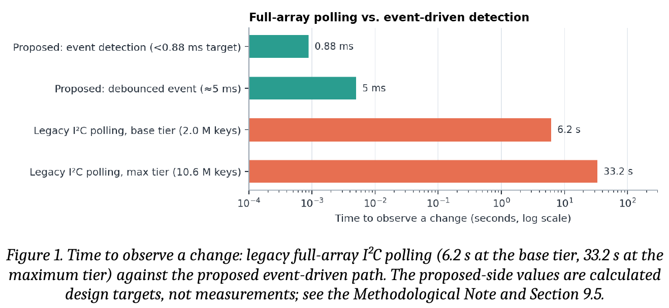
Figure 12. Worst-case service latency when up to 128 sub-matrix modules raise interrupts at the same instant, at 8.5 µs per module; the burst stays well inside the 5 ms confirmation window (Section 10.2.1).
10.3 Next-Generation Interfaces: Beyond I²C-Based Scanning
The source documents propose three specific directions for extending beyond the ceilings identified in Section 10.2, each addressing a different layer of the architecture:
SPI-based expander networks. Replacing the I²C-based expander interconnect examined throughout Chapters 5–6 with Serial Peripheral Interface (SPI) shift-register networks would allow clock rates to increase from the 400 kHz–1.0 MHz range analyzed in Chapters 4–5 to 20 MHz or considerably higher — SPI's point-to-point, full-duplex signaling does not share I²C's open-drain, shared-bus rise-time constraint (Chapter 4, Section 4.4) at all, since each SPI slave typically has its own dedicated chip-select line rather than contending for a shared address space. This would relax the bus-segmentation necessity examined in Chapter 5 considerably, though at the cost of a higher pin count per device (SPI conventionally requires a dedicated chip-select per slave, reintroducing some of the pin-scaling pressure Chapter 2's analysis was specifically designed to avoid) — a genuine architectural trade-off rather than a strict improvement, and one that would need to be evaluated against Chapter 2's pin-efficiency framework rather than assumed superior by clock speed alone.
Parallel multi-lane bus architectures. Rather than a single shared (if segmented) bus hierarchy, dedicated parallel bus topologies — multiple simultaneous physical bus lanes with independent chip-select demultiplexing — would enable genuinely concurrent frame reads across multiple isolated sub-matrices, rather than the time-multiplexed (if fast) sequential branch-activation model examined in Chapter 5. This is architecturally a generalization of the segmentation principle already central to this monograph: where Chapter 5's PCA9546AD switches time-share one physical bus master across many branches, a multi-lane architecture would give multiple branches their own simultaneous physical access, trading additional host-side pin and peripheral cost for genuine parallelism rather than fast time-division.
Custom driver ASICs. The most structurally significant proposed direction is integrating the analog multiplexing (Chapter 3), hardware debouncing (Chapter 7), and delta-generation (Chapter 7) functions directly onto a custom application-specific integrated circuit co-located with the physical matrix substrate, rather than realizing these functions as discrete off-the-shelf components (the CY8C9540A, 74HC4067, and associated logic examined throughout this monograph) connected by PCB-level wiring. This would, in principle, eliminate the discrete-component wiring complexity that motivates much of Chapters 3–4's electrical analysis in the first place, and could push both the trace-length ceiling (Section 10.2) and the achievable scan rate (Chapter 4) considerably further — at the cost of the substantially higher non-recurring engineering investment and lower design flexibility inherent to custom silicon relative to a discrete-component reference design built from commodity parts, the trade-off that has kept this monograph's actual analysis anchored to commodity CY8C9540A/74HC4067/PCA9546AD components throughout.
10.4 Broader Applicability: In-Memory Processing Contexts Beyond the Reference Design
Because this monograph treats the physical switch matrix as one instance of a general sensor-to-in-memory-dataset problem (Section 10.1), the architecture's real applicability is broader than the switch-matrix product context its source documents were originally written around, and it is worth surveying that broader applicability directly in terms of the in-memory processing objective rather than in terms of the human-machine-interface (HMI) product market the underlying hardware happens to be drawn from.
Any application that needs to maintain a very large, sparsely-changing boolean or low-bit-width state space entirely in on-chip memory, updated from a large number of physical or electrical inputs, with computation happening directly against that memory rather than against files, records, or database rows, is structurally the same problem this monograph solves for switch matrices — only the acquisition front-end (Chapters 3–5) changes. Concretely, the design pattern synthesized in Chapter 10.1 (partition the acquisition side, construct the dataset via zero-CPU DMA, compute against it with word-parallel bitwise operations, size the dataset sparsely rather than per-node) generalizes to: real-time sensor-fusion arrays that must maintain a live in-memory occupancy or status map across millions of discrete sensing elements (large tactile or pressure-sensing surfaces, distributed environmental sensor grids) and evaluate that map continuously without ever materializing it as a file; telecommunications and data-center patch-field or port-status monitoring, where the "keys" are physical port or cross-connect states rather than switches, but the requirement — a live, in-memory, bit-per-port dataset updated at interrupt speed and scanned via XOR/CLZ for anomalies — is identical in structure; industrial control and SCADA-adjacent state aggregation, where a very large number of discrete field-device statuses must be reflected into a single in-memory representation fast enough to drive real-time control logic directly against that representation, rather than through a polling database layer; and edge-resident real-time analytics front-ends more generally, where the value of the architecture is precisely that it keeps the entire working dataset in on-chip SRAM (Chapter 9) and therefore never pays the latency cost of a disk, flash, or networked database round-trip on the critical path — the same zero-external-memory property that Chapter 9 establishes for the switch-matrix case.
It is worth being precise about what does and does not transfer to these adjacent domains. The electrical and topological engineering of Chapters 3–5 (the CY8C9540A/74HC4067/PCA9546AD component selection, the specific trace-length and bus-capacitance figures) is specific to the switch-matrix acquisition front-end and would need to be re-derived for a different physical sensing modality — an optical, capacitive, or RF sensing front-end would have entirely different electrical constraints even though it could feed the same downstream in-memory pipeline. What transfers directly, without modification, is the in-memory processing core itself: the zero-copy ping-pong buffer / DMA construction pattern of Chapter 6, the XOR-delta / CLZ in-memory compute pattern of Chapter 7, and the sparse active-allocation memory-sizing discipline of Chapter 9 are all sensing-modality-agnostic and apply unchanged to any large, sparsely-changing boolean dataset that a different acquisition front-end might produce. This is, in fact, the strongest form of the applicability claim this monograph can honestly make: the acquisition engineering is domain-specific, but the in-memory processing architecture is not.
10.5 Concluding Remarks and Deployment Roadmap
This monograph set out to document, reconcile, and critically extend a hardware and firmware architecture capable of constructing and continuously processing, entirely in on-chip memory, a live dataset scaling from roughly 2 million to over 10.6 million discrete state bits, while holding state-update latency in the sub-millisecond-to-low-single-digit-millisecond range (subject to the debounce-timing reconciliation flagged in Chapter 9), host CPU overhead under 2%, and the entire dataset within a few megabytes of on-chip SRAM with no external memory, disk, or database dependency on the real-time path. Three achievements, synthesized across the ten preceding chapters, constitute the core of that result — and each maps directly onto one requirement of the in-memory processing objective stated in this monograph's abstract:
-
Acquisition scaling (feeding the in-memory dataset without a pin explosion). Coupling CY8C9540A I/O expanders with 74HC4067 multiplexers into 288×288, 82,944-key sub-matrix modules, and replicating those modules across a PCA9546AD-segmented bus hierarchy, scales the acquisition front-end from 1.99 million to 10.61 million physical inputs — every one of which becomes a bit in the live in-memory dataset — using a host-side interface of only 32 pins. This is what makes the in-memory dataset's source tractable: a design whose mathematical justification (Chapter 2) and physical realization (Chapters 3–5) are fully traceable to the R=C pin-efficiency result and the practical, PCB-routing-constrained resolution of the M_opt = P/e tensor-optimality result.
-
In-memory dataset construction and computation at effectively constant per-event cost. Transitioning from continuous sequential polling to an interrupt-driven eDMA ingestion pipeline (Chapter 6) that constructs the live dataset with zero CPU involvement, paired with O(1)-per-event ARM Cortex CLZ bitwise scanning (Chapter 7) that computes against that dataset using only in-memory word-parallel operations, reduces active event-detection latency from the legacy baseline of 6.2–33.2 seconds down to the sub-millisecond-to-low-millisecond range, while holding CPU utilization under roughly 2% of a single core — a reduction the source documents variously describe as exceeding 6,200× to 33,200×, and which this monograph's Chapter 9 analysis confirms holds under either of the two internally inconsistent debounce-timing interpretations identified there. This is the achievement most directly answering the in-memory processing objective: it demonstrates that computation against a 10.6-million-node in-memory dataset can be made effectively independent of dataset size.
-
Keeping the entire dataset on-chip. Deploying in-memory XOR delta extraction alongside a sparse active-memory model (Chapter 9) compresses what would otherwise be a 13.28 MB naive per-key debouncing footprint into a 2.671 MB working set — comfortably inside internal zero-wait-state SRAM, avoiding the latency penalty of external memory access entirely for the real-time path. This is the precondition, established last in this monograph but logically first in importance, that makes calling this an in-memory processing architecture rather than a memory-assisted one true in the strict sense: at no point does the live dataset, or any computation against it, leave on-chip SRAM.
Read as a whole, the value of this architecture lies less in any single one of these three achievements and more in their combination: topological scaling alone, without the latency collapse of Chapters 6–7, would still leave the system bottlenecked by sequential polling time; the latency collapse alone, without the memory compression of Chapter 9, would leave the ingestion pipeline correct but memory-constrained at full scale; and neither would be electrically viable at all without the signal-integrity and bus-segmentation groundwork of Chapters 4–5. The architecture's genuine achievement is a consistent engineering discipline — isolate, partition, and charge cost to actual activity — applied without exception across every layer from PCB trace geometry to firmware algorithm, which is what ultimately makes a claim like "10.6 million keys at sub-millisecond latency" a coherent, internally-supported engineering result rather than an assertion resting on any single mechanism alone.
For an organization evaluating deployment of an architecture along these lines, the analysis developed across this monograph suggests a roadmap: validate the sparse active-queue memory model and the debounce-timing parameters explicitly (Chapter 9's flagged inconsistency should be resolved against the actual target hardware's sampling capability before any sub-millisecond latency figure is treated as a firm specification); prototype at the base 24-expander, 1.99-million-key tier first, where thermal, power, and interrupt-servicing margins are widest (Chapter 8, Section 10.2); and treat the 128-expander, 10.61-million-key maximum configuration as the validated ceiling of this specific commodity-component design, pursuing the SPI, parallel-bus, or custom-ASIC extensions of Section 10.3 only if application requirements genuinely demand capacity beyond that point, rather than as a default next step. Within that ceiling, the architecture developed and critically examined across the preceding ten chapters represents a well-reasoned, internally consistent (with the one noted exception) solution to a class of scaling problem that conventional keyboard and industrial-panel design practice was never built to address.
Chapter 11 — Updated Software Strategy: Network-Sourced Binary Workloads Dispatched Across the Expander Fabric
Update notice. This chapter is an update to the monograph, not a separate document. It replaces the switch-scan-only software framing of Chapters 6–7 with the software strategy the author now intends for the hardware, and it records the fundamental engineering questions that strategy raises, together with the best answers the monograph's own hardware analysis supports. The hardware of Chapters 3–5 and 8 (CY8C9540A expanders, 74HC4067 multiplexer trees, PCA9546AD bus switches, i.MX RT host) is unchanged. As throughout this monograph, no figure below comes from built hardware; every number is a calculated design estimate, and every assumption is labeled as one.
11.1 The Updated Software Strategy
The device is connected to the internet over Ethernet. When a prompt is submitted, the host processor requests from the transformer the binary representation of the conversation and the prompt. The binary numbers received are staged on an SD card for processing. The host then sends these numbers, encoded as hexadecimal messages, over the four I²C links — the principal bottleneck of the system — to the CY8C9540A expanders. Because every CY8C9540A owns a dedicated matrix network, the received numbers are split across the matrix networks of many expanders, and the results of processing are returned to the host as messages over the same I²C links.
Each I²C branch holds eight CY8C9540A expanders. When the data assigned to a branch has filled all eight, the chipset signals the host, which switches the bus to the next eight-expander branch and requests further processing. Each matrix network can read and write bits, and the in-memory processing is performed with the help of the CY8C9540A; the central processor is responsible for data mapping, sending and receiving, and splitting the data. In the terminology of this monograph the strategy therefore consists of seven steps, S1–S7, tabulated below with the layer of the existing architecture that carries each step.
| Step | Software action | Carried by (monograph layer) |
|---|---|---|
| S1 | Connect to the internet over Ethernet; exchange the prompt and conversation with the transformer. | Host network stack (new; see Q9) |
| S2 | Request the binary encoding of conversation + prompt from the transformer. | Host application layer (new) |
| S3 | Stage the received binary block on the SD card (SDIO, 4-bit, 50 MHz). | Non-volatile path of Section 6.3 |
| S4 | Map and split the block into hexadecimal frames addressed to (link, branch, expander, row, column). | Host mapper (new; Section 11.4) |
| S5 | Transmit frames over the four I²C links; on branch full, switch the PCA9546AD channel and continue. | Bus layer, Chapter 5; eDMA, Chapter 6 |
| S6 | Bit read/write and bitwise operations inside each expander's matrix network. | Acquisition layer, Chapter 3 (see Q2, Q3) |
| S7 | Return result frames over I²C; reassemble on the host; hand the result back to the network layer. | Ingestion layer, Chapter 6; delta scan, Chapter 7 |
11.2 Fundamental Questions and Answers
The following questions decide whether the strategy is buildable and what it can be expected to achieve. They are ordered from the most fundamental (what computes, what stores) to the most practical (network, security, validation).
Q1. What exactly does the "transformer" return, and where does it run? The strategy says the host requests the binary form of the conversation and prompt from the transformer. Two readings are possible. If the transformer is a remote service reached over Ethernet, the exchange is a token or embedding stream of kilobytes per request, and network round-trip time (tens to hundreds of milliseconds) dominates every microsecond-scale figure in this monograph; the fabric would then process only what the host chooses to hand it. If the transformer is a local model, its weights must live in the system, which raises the capacity question of Q4. Recommendation: define the contract as "remote transformer → fixed-format binary block (token IDs, or a binarized embedding) → fabric," and treat the fabric as a post-processor or similarity engine for that block, not as the place where the transformer itself runs.
Q2. Which component actually performs the computation? The CY8C9540A is a 40-bit I/O expander with I²C access, PWM outputs, interrupt logic and a small EEPROM. It contains no arithmetic or logic unit that can XOR, AND or accumulate data words. In the monograph's own analysis (Appendix A) all bitwise processing — XOR delta extraction and CLZ isolation — executes on the host Cortex-M core, not in the expanders. The strategy sentence "in-memory processing is performed with the help of the CY8C9540A" must therefore be read as: the expander provides addressed access to a bit array, and the computation is performed either by the host on data it has read, or by passive circuit structure in the matrix itself (Q3). Without one of these two, the expanders are storage-and-I/O elements only. Corrected wording adopted in this chapter: the fabric is a distributed, bit-addressable store with host-side bitwise processing; it becomes processing-in-memory in the sense of Appendix A only if compute is added in or beside the cells.
Q3. Can a crosspoint be written, or only read? In the hardware of Chapter 3 each crosspoint is a diode-isolated switch contact. The expander drives a row and senses a column, so a crosspoint can be read but not written: its state is set by the outside world (a contact closing), not by the host. The strategy requires each matrix network to read and write bits. That requires replacing the passive contact with a writable cell — for example a per-crosspoint latch or a gate-charge cell set through the row/column drive, an analog switch whose control state is stored, or a non-volatile resistive element — plus the corresponding redesign of the diode-leakage and RC analysis of Chapters 3–4. This is the single largest open hardware item, and none of the monograph's calculated figures cover it. Until a writable cell is chosen, a write in step S6 can be emulated only by host-side SRAM, which makes the physical matrix redundant (Q4).
Q4. Is there enough capacity to hold a transformer, and what does the fabric add beyond the host SRAM? The maximum fabric is 10,616,832 bits = 1.327 MB. The host already has 5 MB of SRAM (Chapter 9), about 3.95 times that amount, and the monograph's 2.671 MB live footprint is itself a mirror of the fabric. The fabric therefore adds no capacity the host does not already have, and it holds only about 10.6 million one-bit parameters. Table 11-1 puts this against representative models. A 7-billion-parameter language model at 4 bits per weight is roughly 2,600 times too large. Conclusion: the fabric can hold a binary or heavily quantized model of a few million parameters, a hash or embedding index, or a binarized feature block — not a general-purpose language model.
Q5. Is the I²C bandwidth adequate for loading and for running the workload? It is the limiting resource, as the strategy itself notes. Using an explicit transaction model (assumption: one 3-byte write to set row/column address and one 1-byte register read per step, 77 clock cycles, 8 sense bits returned per step, four links operating in parallel, protocol overhead only), a link delivers about 13 kB/s at 1.0 MHz and 5.2 kB/s at 400 kHz. Four links give about 52 kB/s and 21 kB/s. Loading a full 1.327 MB fabric therefore takes about 26 s at 1.0 MHz and 64 s at 400 kHz. Streaming a 4-bit 7B model through the fabric once per generated token would need 3.5 GB per token, or about 19 hours per token at 52 kB/s, whereas reading the same data from the SD card at an assumed sustained 20 MB/s would take about 175 s. The I²C path is thus a poor route for bulk data. Consequence for the strategy: weights or bulk data must be written once and stay resident; only small per-request blocks (kilobytes) should cross the I²C links at run time. The 26 s and 64 s figures use a stricter per-step model than the legacy 6.2 s / 33.2 s figures of Section 1.2 and should be reconciled with them on real hardware.
Q6. How is a binary block mapped to physical bits? The host owns a single flat bit address space. With four links (LPI2C1–4), four PCA9546AD channels per link, eight expanders per channel and 288×288 crosspoints per expander, the global index is G = (((L·4 + C)·8 + E)·82,944) + r·288 + c, where L ∈ 0..3, C ∈ 0..3, E ∈ 0..7, r,c ∈ 0..287. The maximum value is 128 × 82,944 − 1 = 10,616,831, matching Chapter 5. Each 8-bit sense read returns eight columns of one row, so the natural unit of transfer is one byte covering columns 8k…8k+7, and a hexadecimal frame carries whole bytes. The mapper must keep a table of how many bytes each expander holds, so that "full" is a host-side counter rather than a chip-side condition (Q7).
Q7. Who decides that a branch is "full", and how is the switch made safely? A CY8C9540A cannot know that its neighbors are full; it can only raise its interrupt line for a port event. The chipset-to-processor request in the strategy is therefore implemented as host bookkeeping: the mapper counts bytes per expander, and when the eighth expander of a branch reaches capacity it closes the current PCA9546AD channel (write 0x00 to its control register), opens the next (write the channel bit), and resumes. Idle channels stay disconnected, which keeps active-segment capacitance at one branch's worth, as required by Section 5.2. Expander interrupts remain reserved for event notification (Section 5.3). A channel change costs about 20 clock cycles, negligible next to the roughly 0.8 s needed to fill one expander at 1.0 MHz.
Q8. How is data integrity protected? I²C provides only per-byte acknowledgment; it has no error detection for a wrong bit, and a marginal bus can flip data without a NACK. The strategy adds a frame header and CRC-16 over each hexadecimal frame, read-back verification of every written byte during load, and a periodic background scrub that compares a CRC of each expander's image with a host copy. SD-card blocks should carry their own CRC. Bus-lock recovery follows Section 5.4.
Q9. How does the device reach the network? The i.MX RT500 family named in the bill of materials (MIMXRT555) lists USB, SDIO/eMMC, FlexComm (UART/SPI/I²C) and I3C peripherals but no on-chip Ethernet MAC, and its Cortex-M33 is specified at up to 275 MHz rather than the 500 MHz used in Chapter 9's CPU-load target (that target should be re-derived at 275 MHz). Ethernet therefore needs an external controller on SPI (for example a hardwired-TCP/IP part) or a different host. TLS to a remote service also needs certificate storage and roughly 100 kB or more of working RAM, competing with the 2.671 MB fabric mirror for the 5 MB SRAM budget.
Q10. Is the SD card the right staging medium? For a prompt-sized block (kilobytes) SRAM is sufficient and faster; the SD card is justified for persistence — logging, resumable loads, model images — not as a required hop. Placing SD in the critical path adds tens of milliseconds of write latency and card wear without benefit. The SD card should be kept as an optional write-behind path (Section 6.3) and the primary staging buffer should be the ping-pong SRAM of Chapter 6.
Q11. Which workloads actually fit a bit-addressable, host-side bitwise engine? Workloads whose cost is dominated by wide bit operations on a small, resident dataset: binary or ternary neural layers (XNOR + population count), Hamming-distance similarity search over binarized embeddings, hashing and Bloom-filter membership, and sparse-event detection (the original XOR/CLZ path). The Cortex-M33 has CLZ but no population-count instruction, so popcount must be built from table lookup or bit-parallel arithmetic, and the cost per 32-bit word should be measured before any throughput claim is made.
Q12. What are the privacy, power and validation consequences? Conversation text staged on removable media is data at rest; the RT500's AES and secure-boot features should encrypt it and the SD card should not hold plaintext. Power stays within the 4.2 W budget of Chapter 8 only if simultaneous switching of all branches is not required, which the sequential branch model guarantees. Validation must begin at the smallest possible scale (Section 11.5).
11.3 Capacity Against Representative Models
Table 11-1. Fabric capacity (10,616,832 bits) against model size at several precisions (calculated). A ratio above 1 means the model does not fit.
| Model (parameters) | 1 bit / weight | 4 bits / weight | 8 bits / weight |
|---|---|---|---|
| Fabric capacity | 10.6 M params | 2.65 M params | 1.33 M params |
| BERT-base (110 M) | 10.4× too large | 41× too large | 83× too large |
| GPT-2 small (124 M) | 11.7× too large | 46.7× too large | 93.4× too large |
| 7 B-parameter LLM | 659× too large | 2,637× too large | 5,275× too large |
Table 11-2. I²C throughput and load time under the Q5 transaction model (77 clocks per 8-bit step, 4 links in parallel; calculated).
| Bus clock | Per link | 4 links | One expander (82,944 bits) | Full fabric (128 expanders) |
|---|---|---|---|---|
| 400 kHz Fast-Mode | 5.2 kB/s | 20.8 kB/s | 2.0 s | 63.9 s |
| 1.0 MHz Fast-Mode Plus | 13.0 kB/s | 51.9 kB/s | 0.80 s | 25.5 s |
11.4 Updated Software Architecture
The software is organized in four cooperating tasks on the host, each mapped onto an existing layer so that the eDMA and ping-pong machinery of Chapter 6 is reused rather than replaced.
| Task | Responsibility | Existing mechanism reused |
|---|---|---|
| Network task | Ethernet, TLS, request/response with the transformer; produces a binary block. | None (new; external MAC, Q9) |
| Mapper / splitter | Convert the block to hexadecimal byte frames; compute G from Q6; track bytes per expander and per branch. | Scatter-gather descriptors, Section 6.2 |
| Bus scheduler | Select PCA9546AD channel, issue frames on the four LPI2C links, handle NACK/CRC retries, switch branch on fill. | Bus layer, Chapter 5; lock recovery, Section 5.4 |
| Result collector | Read result bytes back, verify CRC, reassemble, pass to the network task. | Ping-pong buffers, Section 6.3; XOR/CLZ scan, Chapter 7 |
Every I²C frame follows one layout, so that the mapper, the scheduler and the collector share a single definition:
| SOF | SEQ(16) | L(2) C(2) E(3) | OP(4) | ROW(9) | COL8(6) | LEN(8) | PAYLOAD(hex bytes) | CRC16 |
OP: 0=WRITE_BYTES  1=READ_BYTES  2=XOR_ROW  3=SCRUB  4=STATUS
Flow: block -> hex frames -> [select channel] -> send -> verify(read-back) -> next expander
      -> branch full? -> deselect channel, select next -> ... -> results -> CRC check -> reassemble
Branch switching follows the sequence of Q7. Frames are queued per link, so the four links transfer in parallel and only one PCA9546AD channel per link is ever open, preserving the capacitance isolation of Chapter 5.
11.5 Verdict and Roadmap
What the strategy can achieve. As a distributed, bit-addressable store fed from the network, with host-side bitwise processing and event-driven result return, the strategy is buildable with the existing bus architecture. It suits binary or small quantized models, Hamming-space search, and filtering of binary blocks received from a remote transformer.
What it cannot achieve as stated. It cannot host a large language model in the fabric (Table 11-1), cannot stream bulk weights over I²C at useful speed (Table 11-2), and cannot perform in-expander computation with the CY8C9540A, which has no logic unit. The crosspoints must also be redesigned before they can be written.
Recommended next steps, in order. (1) Fix the role of the transformer (Q1). (2) Choose and characterize a writable crosspoint cell on one 288×288 sub-matrix (Q3). (3) Build one PCA9546AD branch with eight expanders and measure the real per-step transaction time against Table 11-2. (4) Implement the Section 11.4 frame format with CRC and read-back on that branch. (5) Add the external Ethernet controller and reconcile the host clock and SRAM figures (Q9). (6) Only then scale to more branches. Chapter 10.5's recommendation to prototype at the base tier before treating any figure as a specification applies to this chapter without change.
11.6 Consequences for Earlier Chapters
The Abstract and Framing Note describe the system as an in-memory processing platform; with this update that description is qualified as follows. The host executes the bitwise processing, and the expanders provide addressed access (Q2); Appendix A's classification of the design as neither PNM nor PUM therefore stands unchanged. Chapter 6's non-volatile path is extended from event logging to optional staging (Q10). Chapter 9's CPU-load target and SRAM budget must be re-derived for the 275 MHz core and the network stack (Q9). Chapter 3's crosspoint description applies to the acquisition use case only; the read/write use case of this chapter requires the cell redesign of Q3.
Chapter 12 — Dual-Port SRAM at the Matrix Layer: Architecture, Timing, and Hazard Management
Update notice. This chapter extends the monograph by analyzing dual-port SRAM for the live state array of Chapters 6 and 9. The hardware of Chapters 3–5 and 8 is unchanged. As throughout this monograph, no figure below comes from built hardware: every number is an exact arithmetic consequence of the geometry, a result of the accompanying behavioral simulation (a cycle-level model, not RTL synthesis), or a calculated estimate whose assumptions are labeled.
12.1 Objective and Position in the Architecture
The four layers of Chapters 3–7 are unchanged. Only the boundary between the ingestion layer (Chapter 6) and the algorithmic layer (Chapter 7) is affected: the live array GLOBAL_STATE_BITMAP of Section 9.1, which the single-port design protects with a ping-pong pointer swap, becomes a dual-port array with a write port fed by the eDMA engine and a read port used by the XOR/CLZ stage.
eDMA (TCD chain) --> PORT A (write, 32 b) --+
                                            |    STATE ARRAY 331,776 x 32 b
                                            +-- K word-interleaved banks
                                            |   + dirty tags + undo log
XOR / CLZ delta stage <-- PORT B (read, 32 b)
Four memory organizations are compared throughout the chapter.
| Organization | Ports and cell | Same-address, same-cycle behaviour |
|---|---|---|
| Single-port (SP, 1RW) | one shared port, 6T | impossible; serialized by an arbiter |
| Banked single-port (BANK-K) | one port per bank, 6T | conflict only within one bank; serialized |
| Pseudo-dual-port (PDP, 1R1W) | one read and one write port, 8T | read returns old data unless bypassed |
| True dual-port (TDP, 2RW) | two independent read/write ports, 8T-class | write/write undefined; read/write depends on macro mode |
Platform note. The dual-port analysis applies to an FPGA or custom-silicon realization. A commercial MCU exposes a fixed SRAM whose TCM is multi-mastered through a crossbar, not a selectable dual-port macro. On an FPGA, whose block RAM is natively true dual-port (AMD UG573), the mapping is exact: 10,616,832 bits equal 324 × 32,768, that is 324 block RAMs of 32 Kb data capacity, a consequence of the 288² × 128 geometry. The 5.0 MB SRAM figure used in Chapter 9 should also be re-verified against the reference manual of the selected part, because the smaller Teensy-class devices carry roughly 1 MB.
12.2 Array Organization and Port Assignment
Let N_b = 10,616,832 state bits and W = 32 bits per word, so N_w = N_b/W = 331,776 words. The array is split into K = 32 word-interleaved banks (bank = address mod 32) of 10,368 words (41,472 B) each, so that sequential eDMA bursts and sequential sweeps fall on different banks in successive cycles and each bank fits one macro.
Port A is dedicated to ingestion. It writes 32 bits with byte enables, so one expander port byte updates eight nodes without a read-modify-write that would otherwise occupy the read port. Port B is dedicated to evaluation and feeds the XOR delta stage of Chapter 7. Even in a true dual-port macro the ports are dedicated in this way, which reduces the collision surface to same-address read/write pairs.
Three auxiliary structures support consistency (Section 12.6): an epoch register E incremented at each snapshot boundary; one dirty bit per 256-word granule (1,296 bits), which also lets the reader skip clean granules; and an undo log of 16 K entries × 48 bits (96 KB). With the undo-log protocol the previous-frame shadow bitmap of Section 9.1 (1.327 MB) is no longer needed, so the total is 1.42 MB against 2.65 MB for the dual-bitmap ping-pong scheme.
12.3 Mathematical Foundations
Notation. f is the clock frequency (500 MHz reference); ρ is the writer duty cycle (write accesses per cycle); c is the reader issue interval in cycles per word (c = 2 in Section 12.8); L is the write-burst length in words (L = 4).
Bandwidth. One 32-bit port at 500 MHz moves BW_port = W·f/8 = 2.0 GB/s. A single-port array is feasible only if r + w ≤ 1 for read demand r and write demand w (accesses per cycle); a dual-port array requires only max(r, w) ≤ 1. The throughput speedup is
$$S = (r + w) / \max(r, w) \le 2, \text{ with equality iff } r = w \tag{12.1}$$
A reader-limited sweep (r = 1/c) saturates a single port when ρ ≥ 1 − 1/c, that is at ρ = 0.5 for c = 2.
Ingest ratio. A 1 MHz Fast-Mode-Plus bus delivers at most 1 MHz / 9 clocks per byte ≈ 111 kB/s; four LPI2C links give ≈ 444 kB/s, or 111,000 words/s. Hence
$$\rho_{in} = 111{,}000 / (500 \times 10^6) \sim 2.2 \times 10^{-4} \tag{12.2}$$ $$\text{BW\_port / BW\_ingest} = 2.0\ \text{GB/s} / 444\ \text{kB/s} \sim 4{,}500$$
For the I²C-fed architecture, memory bandwidth is therefore not the bottleneck by more than three orders of magnitude.
Single-port stall model. With writer priority, a reader access that arrives while a burst of L cycles is in progress waits for its remainder. For random arrivals the mean stall is
$$s_{SP} \sim \rho (L + 1) / 2 \text{ cycles per access} \tag{12.3}$$ $$N_w \cdot c \le T_{sweep,SP} \le N_w \cdot c / (1 - \rho) \tag{12.4}$$
The worst-case wait is L cycles for isolated bursts but is bounded only by the write-queue depth under sustained ingest (4,140 cycles at ρ = 0.9 in Section 12.8). For K word-interleaved banks and sequential streams, the fraction of reader cycles lost to bank conflicts is
$$f_{stall,BANK}(K) = \rho / (c K) \tag{12.5}$$
Simulation reproduces (12.5): at ρ = 0.5 and c = 2, K = 4 gives 0.0625 (predicted 0.0625) and K = 8 gives 0.0312 (predicted 0.03125), each conflict costing one cycle.
Pipeline effect (Hennessy and Patterson, 2017). For base CPI₀ and a fraction m of instructions addressing the array, the relative CPI reduction from removing port conflicts is
$$dCPI / CPI_{SP} = m \cdot s_{SP} / (CPI_0 + m \cdot s_{SP}) \tag{12.6}$$
For m = 0.3, CPI₀ = 1.2, ρ = 0.25, L = 4 this is 13.5%; at ρ = ρ_in it is 0.014%.
Event-to-visible latency. From the moment the eDMA holds the expander byte to the moment the word is readable on port B:
$$T_{vis} = t_{arb} + t_{write} + t_{sync} \tag{12.7}$$ $$\text{DP: } t_{arb} = 0,\ t_{write} = L\ \text{cycles},\ t_{sync} = 1 \to 5\ \text{cycles} = 10\ \text{ns at 500 MHz}$$
The I²C transaction that precedes this (at least 72 µs = 36,000 cycles for an eight-byte read) is about four orders of magnitude longer, so memory-side latency does not determine the end-to-end figure of Section 9.3.
Area (Weste and Harris, 2011). The array area is A(X) = N_b · a_cell(X) / η, and α = a_8T / a_6T lies typically between 1.3 and 1.8. With the illustrative assumptions a_6T = 0.127 µm² (representative high-density 28 nm cell), array efficiency η = 0.70 and α = 1.5, the 6T macro occupies 1.926 mm² and the 8T macro 2.889 mm² (+0.96 mm², +50%). If the shadow bitmap is removed, one 8T array plus undo log (≈ 3.1 mm²) is smaller than a 6T ping-pong pair (2 × 1.926 = 3.85 mm²). This is the strongest area argument for dual-port here, and it depends on the protocol of Section 12.6, not on the macro.
Power and energy-delay product. With E_frame = N_acc·E_acc + P_leak·T_frame and EDP = E_frame·T_frame, we assume a dynamic-energy ratio E_DP/E_SP = 1.15, a leakage ratio of 1.4, and a single-port frame energy split 80% dynamic, 20% leakage at ρ → 0. Using the simulated single-port sweep-time ratio σ = T_SP / T_0:
| ρ | σ | EDP_SP | EDP_DP | EDP_DP / EDP_SP |
|---|---|---|---|---|
| 0.001 | 1.001 | 1.00 | 1.20 | 1.20 |
| 0.05 | 1.046 | 1.06 | 1.20 | 1.14 |
| 0.25 | 1.291 | 1.37 | 1.20 | 0.88 |
| 0.50 | 1.875 | 2.20 | 1.20 | 0.55 |
| 0.90 | 8.92 | 23.0 | 1.20 | 0.05 |
The crossover lies at ρ* ≈ 0.15. With a dynamic ratio of 1.05 and a leakage ratio of 1.2 it falls to ≈ 0.07; with 1.3 and 1.6 it rises to ≈ 0.25. The conclusion that ρ_in ≈ 2.2 × 10⁻⁴ lies far below any plausible crossover is robust; the crossover value itself is not.
12.4 What Dual-Port SRAM Guarantees
Dual-port SRAM guarantees that a 32-bit word is never read half-written. That property belongs to the cell array and sense path; it says nothing about consistency across words. Simultaneous writes to one address are undefined in a true dual-port macro, and a simultaneous read and write returns old data, new data, or an indeterminate value depending on the read-during-write mode, so an arbiter or bypass is required (Section 12.5).
Frame-level tearing is unaffected by port count. A full sweep takes at least N_w·c = 663,552 cycles (1.33 ms at 500 MHz), and any burst landing inside that window can be observed half-applied; Table 12.4 shows torn events under every memory organization. Frame consistency is a protocol property. Likewise, the state vector supplied to a language model at the top of the pipeline removes staleness and tearing as error sources, but it cannot by itself eliminate hallucination; any such rate must be measured on the deployed model.
12.5 Bus Synchronization and Hazard Management
| Hazard | Definition at the matrix layer | Resolution |
|---|---|---|
| RAW | reader expects the value written in the same or preceding cycle | write-to-read bypass (below) |
| WAR | writer overwrites a word the reader was assigned but has not consumed | undo log or epoch snapshot (12.6) |
| WAW | two writers reach one address | single write port; address-range ownership per TCD chain |
| Structural | two requests need one port | arbiter (SP) or dual port |
| Multi-word (torn) | an event spans several words | commit window or epoch tags (12.6) |
RAW bypass (pseudo-dual-port, registered read). In a synchronous 1R1W SRAM a write at cycle k is visible to a read presented at cycle k + 1; a same-cycle read of the same address returns the old value. A bypass forwards the write data:
reg [31:0] wr_data_q; reg [18:0] wr_addr_q, rd_addr_q; reg wr_v_q;
always @(posedge clk) begin
  wr_data_q <= data_a;  wr_addr_q <= addr_a;  wr_v_q <= we_a;
  rd_addr_q <= addr_b;
end
wire raw_hit = wr_v_q && (wr_addr_q == rd_addr_q);
assign q_b   = raw_hit ? wr_data_q : mem_q;   // one comparator, one mux
The cost is a 19-bit comparator, a 32-bit 2:1 multiplexer on the read data path and 51 flip-flops; register q_b if the read path is critical and add one pipeline cycle to (12.7).
True dual-port collision policy. Recommended: write wins, the read replays one cycle later and observes the new data.
wire collide = we_a && re_b && (addr_a == addr_b);
assign busy_b = collide;       // reader holds and retries
The alternatives are read-first (no stall, stale-by-one-event data) and the bypass above. Collisions are rare (0–17 per run of up to 2.7 × 10⁷ cycles in Table 12.4), so the policy costs at most one reader cycle each.
Single-port arbiter (reference). Fixed priority with writer first: grant_w = req_w; grant_r = req_r & ~req_w. The reader delay is unbounded under sustained ingest, so a credit limit is added: after C_max consecutive writer grants, one reader grant is forced and the write FIFO absorbs the delay.
Cycle-level timing. A write and a read of the same address X in cycle 0 behave as follows.
PDP, read-first :  q_b @1 = OLD(X)      q_b @2 = D1
PDP + bypass    :  q_b @1 = D1          q_b @2 = D1
TDP, policy 1   :  busy_b @0 = 1; read reissued @1  ->  q_b @2 = D1
12.6 Frame-Consistent Snapshots
The objective is a snapshot in which every multi-word event is present entirely or absent entirely, without ever stalling the writer.
Protocol P1 (commit window). Events queue in a FIFO during the sweep and are applied between sweeps, followed by epoch++. Tearing is eliminated by construction, but event-visible latency grows to about one sweep plus the commit (Table 12.5), and because sweep and commit never overlap, P1 gives dual-port no advantage over single-port. It serves as the correctness baseline.
Protocol P2 (epoch-tagged undo log). The reader snapshots at epoch E. When the writer modifies a word for the first time in E, it first appends (address, old value) to the log; the reader takes the logged value for any dirty word and the array value otherwise.
ingest_word(a, v):                          // writer, port A
  if first_write_in_epoch(a):
      log_push(a, mem[a]); dirty[a>>8] = 1
  mem[a] = v

read_snapshot(a):                           // reader, port B
  if dirty[a>>8] and (i = log_find(a)) >= 0: return log[i].old
  return mem[a]

epoch advance: clear dirty tags, reset log pointer, E++
Log occupancy equals the number of distinct words written during one sweep. Table 12.6 gives the simulated maximum: 4.4 × 10² words at ρ = 0.001 and 1.7 × 10⁴ at ρ = 0.05. For the I²C-fed configuration this scales to under about 100 entries, so the 16 K-entry log has more than two orders of magnitude of margin; for ρ ≥ 0.25 the log must be enlarged to 2¹⁷–2¹⁸ entries or the snapshot period shortened. The lookup cost is the real constraint: a content-addressable memory (Pagiamtzis and Sheikholeslami, 2006) per read is prohibitive, so lookups are limited to dirty granules and use a hashed SRAM. Correctness follows from three facts: the reader sees, for each word, either the never-modified value or the logged pre-epoch value, both equal to memory at the epoch boundary; first-write-per-epoch prevents later writes from overwriting the logged value; and an event is therefore seen wholly before or wholly after the boundary, the multiversion idea of concurrent reading and writing (Lamport, 1977) realized with a bounded log.
Ownership and caching. Each TCD chain owns a disjoint address range (removing WAW). If port B is fronted by a D-cache, the targeted invalidation of Section 6.3 must cover each granule read, and with P2 the array and log should be placed in non-cacheable or write-through memory.
12.7 Power, Performance and Area Trade-off Matrix
Area and EDP entries (†) depend on the assumptions of Section 12.3; stall, sweep and tearing entries come from the simulation of Section 12.8.
| Organization | Array area † | Reader stall, ρ = 0.5 | Max stall run | Sweep time, ρ = 0.5 | EDP vs SP † | Torn frames without protocol |
|---|---|---|---|---|---|---|
| SP 1RW (6T) | 1.93 mm² | 46.7% | 151 cycles | 1.244 M | 1.00 | yes |
| BANK4 (6T) | ≈ 2.1 mm² (+10%) | 6.25% | 2 | 0.708 M | ≈ 0.5 | yes |
| BANK8 (6T) | ≈ 2.2 mm² (+15%) | 3.12% | 2 | 0.685 M | ≈ 0.5 | yes |
| PDP 1R1W (8T) | 2.89 mm² | 0% | 0 | 0.664 M | 0.55 | yes |
| TDP 2RW (8T) | ≈ 3.0–3.2 mm² | ≈ 0% | 1 | 0.664 M | ≈ 0.55 | yes |
Below ρ ≈ 0.15, single-port or banked single-port wins on EDP and area, and the I²C-fed baseline (ρ_in ≈ 2.2 × 10⁻⁴) lies deep in this region. Between 0.15 and about 0.5, dual-port and banked 6T perform comparably; banked 6T is smaller, while dual-port offers strictly zero-stall behaviour and simpler worst-case timing analysis. Above about 0.5 single-port saturates (stall fraction 0.89 at ρ = 0.9). Against banked 6T the sweep-time advantage of dual-port is only 6–13% at ρ = 0.9, so its remaining advantages are determinism and, with P2, removal of the shadow bitmap. Leakage can be reduced by power-gating clean granules using the dirty-tag map, but no figure has been derived.
12.8 Simulation Results
Method. A cycle-level behavioural model (hca_memory_sim.c) drives one writer, issuing bursts of L = 4 consecutive words at uniform random base addresses with probability ρ/L per cycle, and one reader sweeping all 331,776 words in ascending order at one request per c = 2 cycles. It models the five organizations of Section 12.1 (writer priority on conflict; PDP reads before write on same-address collisions; TDP stalls the reader one cycle), with protocols P0 (unprotected) and P1 (commit window), over 40 sweeps for ρ < 0.5 and 4 sweeps otherwise. It treats each access as single-cycle and models neither physical timing nor power. A first run with c = 1 showed no tearing in PDP/TDP; that was an artifact of reader and writer moving in lock-step, so only c = 2 results are reported, and any RTL testbench must likewise avoid equal access rates.
Table 12.3 — Mean sweep time (cycles; multiply by 2 ns at 500 MHz)
| ρ | SP | BANK4 | BANK8 | PDP | TDP |
|---|---|---|---|---|---|
| 0.001 | 664,131 | 663,631 | 663,593 | 663,551 | 663,551 |
| 0.05 | 694,148 | 667,717 | 665,639 | 663,551 | 663,551 |
| 0.25 | 856,966 | 684,916 | 674,085 | 663,551 | 663,551 |
| 0.50 | 1,244,198 | 707,793 | 684,927 | 663,551 | 663,552 |
| 0.90 | 5,917,053 | 747,835 | 703,156 | 663,551 | 663,552 |
The single-port values lie inside bracket (12.4) (for example [663,552; 1,327,104] at ρ = 0.5), and PDP/TDP sit within one cycle of the lower bound N_w·c.
Table 12.4 — Stalls, collisions and tearing (P0)
| Memory | ρ | Reader stall fraction | Max stall run | Max event write latency | Collisions | Torn events / sweep |
|---|---|---|---|---|---|---|
| SP | 0.05 | 0.044 | 20 | 12 | 0 | 0.15 |
| SP | 0.50 | 0.467 | 151 | 36 | 0 | 1.25 |
| SP | 0.90 | 0.888 | 4,140 | 166 | 0 | 10.75 |
| BANK8 | 0.50 | 0.031 | 2 | 33 | 0 | 0.25 |
| BANK8 | 0.90 | 0.056 | 2 | 167 | 0 | 0.75 |
| PDP | 0.25 | 0.000 | 0 | 24 | 17 | 0.30 |
| PDP | 0.50 | 0.000 | 0 | 37 | 6 | 1.50 |
| TDP | 0.25 | 0.000 | 1 | 23 | 11 | 0.15 |
| TDP | 0.90 | 0.000 | 1 | 137 | 5 | 1.25 |
Tear counts are small-sample estimates (1–10 events per configuration), so only their order of magnitude and the fact that dual-port does not remove tearing should be drawn from them; the expected number per fixed-length sweep is about ρ(L−1)/L. Maximum write latency is set by writer queueing and barely differs between memory types: the read side, not the write side, is the differentiator.
Table 12.5 — Protocol P1: event-visible latency (cycles)
| Memory | ρ | Mean | Max | Torn events |
|---|---|---|---|---|
| SP | 0.001 | 331,589 | 664,107 | 0 |
| PDP | 0.001 | 334,611 | 664,172 | 0 |
| SP | 0.25 | 548,900 | 886,397 | 0 |
| PDP | 0.25 | 549,039 | 886,702 | 0 |
| SP | 0.90 | 1,343,191 | 1,798,504 | 0 |
| PDP | 0.90 | 1,340,406 | 1,795,771 | 0 |
P1 is indistinguishable between SP and PDP, as predicted. Mean visibility is 0.66 ms at ρ ≈ 0 and 2.7 ms at ρ = 0.9, so the sub-0.88 ms detection target of Section 9.3 is met only through the event-driven path of Chapter 7; full-frame sweeps (1.33 ms) serve as integrity scans, not as the primary detection path.
Table 12.6 — Maximum distinct words written per sweep (undo-log demand)
| ρ | SP | BANK8 | PDP | TDP |
|---|---|---|---|---|
| 0.001 | 440 | 460 | 444 | 404 |
| 0.05 | 17,531 | 16,658 | 16,875 | 17,049 |
| 0.25 | 95,160 | 74,566 | 74,175 | 74,124 |
| 0.50 | 210,825 | 132,516 | 130,815 | 131,157 |
| 0.90 | 331,743 | 201,088 | 197,323 | 197,861 |
Synthesis. No synthesis or place-and-route was run, so the area, power and EDP results above remain estimates. The minimum credible follow-up is RTL for the bypass, arbiter, epoch tags and hashed log; an RTL testbench with non-lock-step access reproducing Tables 12.3–12.6; FPGA place-and-route on a device with at least 324 block RAMs, reporting resource counts, read-path Fmax with and without the bypass, and vendor power estimates; and, for silicon, memory-compiler characterization of 6T 1RW, 8T 1R1W and 8T 2RW macros at 64 KB granularity.
12.9 Limitations and Conclusions
The simulation assumes uniform random burst placement and a fixed L = 4, whereas real sensor activity is clustered in space and time and raises local collision and dirty-granule rates; real 8T macros may have different read and write latencies from the single-cycle model; and all area, power and EDP values are parametric. These limits affect the crossover value but not its direction.
Dual-port SRAM at the matrix layer offers zero-stall, bounded-latency access and up to 2× peak bandwidth, and with an epoch-tagged undo log it can reduce total silicon relative to ping-pong buffering. It does not provide frame-consistent snapshots by itself, and for the I²C-fed design of this monograph, where ingest uses about 0.02% of memory bandwidth, it does not repay its area and leakage on throughput or EDP grounds. The recommended path is to retain the single-port ping-pong design for the I²C baseline; to adopt banked 6T if contention ever matters; and to adopt 1R1W dual-port with protocol P2 for parallel-ingest FPGA or ASIC variants (ρ ≳ 0.15) or wherever hard worst-case bounds are required. The literature relied on in this chapter is listed as items [32]–[36] of the References.
Overall Conclusion
This monograph asked how a very large, sparsely changing external state space, up to 10,616,832 discrete switch crosspoints, can be acquired, ingested and evaluated as a live dataset that never leaves on-chip SRAM. Its answer is a four-layer architecture in which every layer applies the same rule: charge cost to what actually changes, not to the total size of the array. The conclusions below follow the chapters in order.
Why the problem needs an architecture, not a faster clock (Chapters 1–2). Sequential polling scales linearly with node count, about 6.2 s for the 1,990,656-node base tier and 33.2 s for the maximum configuration over a 400 kHz I²C bus, and a direct pin-per-switch mapping is physically impossible. The mathematical analysis shows that a two-dimensional layout is the practical optimum: the R = C result gives the pin-efficient shape, and the M_opt = P/e argument explains why higher-dimensional addressing is not worth the routing cost on a PCB.
Acquisition, signal integrity and bus (Chapters 3–5). CY8C9540A expanders and 74HC4067 multiplexer trees form 288×288 sub-matrix modules of 82,944 crosspoints each (a 57.6× pin compression), and 128 modules reach the full 10,616,832 nodes behind a host interface of 32 pins. Partitioning shortens the electrical paths, with settling time falling from 287.28 ns to 18.40 ns and allowing a 10 MHz scan clock, and PCA9546AD switches isolate the bus into branches that reuse addresses and keep active capacitance below 100 pF against the 400 pF limit. Interrupts from the expanders replace polling.
Ingestion and in-memory computation (Chapters 6–7). LPI2C FIFO triggers, DMAMUX routing, scatter-gather descriptors and ping-pong SRAM buffers build the live dataset without CPU polling. XOR delta extraction followed by the ARM CLZ instruction then isolates each changed bit at constant cost per event. The software model of Chapter 9 confirmed this behaviour: every trial reproduced the injected changes exactly, with word reads constant at 331,776 and CLZ operations equal to the number of changed bits.
Power, reliability and memory (Chapters 8–9). The design targets a peak draw below 4.2 W, and the FMEA and bill of materials show what a build would require. The sparse active-allocation model cuts a naive 13.28 MB per-key debouncing footprint to 2.671 MB, 53.42% of the 5.0 MB on-chip SRAM. The resulting targets are event-detection latency below about 0.88 ms (roughly 5 ms once the full debounce is included) and host CPU load below 1.9%, which is the source of the 6,200× to 33,200× improvement over polling.
Extensions (Chapters 11–12). The network-sourced workload strategy is buildable as a distributed, bit-addressable store with host-side bitwise processing, and it suits binary or small quantized models and Hamming-space search. It cannot host a large language model (a 7-billion-parameter model is 659 times too large even at one bit per weight), it cannot move bulk weights over I²C at useful speed (about 20.8 to 51.9 kB/s over four links), the CY8C9540A has no logic unit for in-expander computation, and the crosspoint cell must be redesigned before it can be written. The dual-port SRAM study finds that dual ports give bounded, zero-stall access and up to 2× peak bandwidth but no frame-consistent snapshots by themselves. Because I²C ingest uses only about 0.02% of memory bandwidth, they do not repay their area and leakage in this design: single-port ping-pong stays the baseline, banked 6T is the fallback if contention appears, and 1R1W dual-port with protocol P2 is reserved for parallel-ingest FPGA or ASIC variants. Appendix A places the whole design outside the processing-in-memory categories (neither PNM nor PUM) while sharing the goal of minimizing data movement.
What the result is worth. No single mechanism carries the claim. Topological scaling without the latency collapse would still be limited by polling time; the latency collapse without the memory compression would be correct but memory-bound at full scale; and neither would be electrically viable without the signal-integrity and bus work. The in-memory core (zero-copy ping-pong ingestion, XOR/CLZ evaluation, sparse memory sizing) does not depend on switch sensing and transfers to any large, sparsely changing boolean dataset.
Limits that must stay attached to it. No prototype has been built at any tier, so every figure is an analytically derived design target. The consistency checks found two discrepancies: the Chapter 4 delay table does not support the quadratic-delay narrative, and the 8.3 µs scan is a per-module cost, not a full-array sweep, which is bounded below by about 0.66 ms. The debounce timing also had to be reconciled between the sub-millisecond and roughly 5 ms interpretations. The improvement ratios compare against the weakest plausible baseline, not against dedicated scan controllers, FPGA scanners or an ASIC, and the CPU-load and SRAM figures must be re-derived for the 275 MHz core and network stack of Chapter 11. The contribution is therefore the worked, cross-checked design, the observation that no established design addresses this density, and the design-pattern argument, and it is no larger than that.
Next steps. Build and measure the base tier first (24 expanders, 1.99 million nodes), where thermal, power and interrupt margins are widest, alongside a SPICE model of one sub-matrix bank. Validate the sparse-queue model and the debounce parameters on that hardware, and for the Chapter 11 use case characterize a writable crosspoint cell and measure real per-step I²C transaction times on one eight-expander branch. Treat the 128-expander, 10.6-million-node configuration as the ceiling of this commodity-component design, and turn to SPI, parallel-bus or custom-ASIC extensions only if requirements demand more.
Appendix A — Positioning Against Processing-in-Memory (PIM) and Near-Memory Computing Literature
Chapter 10 argued that this architecture's in-memory processing core (Chapters 6, 7, and 9) generalizes beyond the switch-matrix domain. That claim is sharpened considerably by situating the architecture against the academic and industrial literature that uses the term "in-memory processing" in its more established, narrower sense — processing-in-memory (PIM) and near-memory computing research — because doing so clarifies exactly which category of system this monograph's architecture belongs to, and, just as importantly, which category it does not.
A.1 The PIM/PNM/PUM Taxonomy
The processing-in-memory literature draws a standard architectural distinction between two families of approach. Processing-Near-Memory (PNM) designs place a general-purpose or application-specific processing element physically adjacent to a memory array — in the logic layer of a 3D-stacked memory, at a DRAM bank's peripheral circuitry, or in a memory controller — so that computation happens close to the data without the data itself being manipulated by the memory cells. Processing-Using-Memory (PUM), by contrast, exploits the analog electrical properties of the memory cells themselves (for instance, driving multiple DRAM rows simultaneously to perform a bulk bitwise operation as a side effect of the cells' own charge-sharing physics) to perform computation in situ, without a separate logic element at all. Commercial and research PIM systems — UPMEM's DDR4-based near-bank PIM, Samsung's HBM-PIM, SK Hynix's GDDR6-AiM — are near-memory designs in this taxonomy: each places a modest processing core adjacent to a memory bank to exploit that bank's internal bandwidth, which is otherwise inaccessible to a host CPU sitting across a shared, comparatively narrow memory bus.
Read against this taxonomy, the architecture developed across this monograph is a near-memory processing design in spirit, but not in the literature's strict architectural sense, and the distinction is worth stating precisely rather than glossing over. Chapter 7's CLZ-based delta scanning executes on the same ARM Cortex host CPU that also runs the rest of the system's firmware — it does not run on a dedicated processing element physically integrated into the SRAM array the way a PNM design's near-bank core is integrated into a DRAM bank, nor does it exploit any analog cell-level physics the way a PUM design does. What this architecture does share with the PIM literature's motivating concern is the underlying goal: minimizing data movement between where data is acquired and where it is computed upon. Chapter 6's zero-copy ping-pong buffering and Chapter 7's in-place bitwise operations both exist specifically to avoid the "data movement bottleneck" that the PIM literature identifies as processing-in-memory's central justification — the observation, consistent across the research surveyed here, that the performance and energy cost of moving data between memory and a processor increasingly dominates the cost of the computation performed on that data once it arrives, particularly for workloads (like this architecture's XOR/CLZ delta scanning) that are simple per-datum but touch very large datasets.
A.2 Where This Architecture Sits, and Why That Placement Is the Right One for Its Objective
The precise classification, then, is that this monograph's architecture is a CPU-adjacent, tightly-coupled-memory (TCM) in-memory processing design: it is calculated to achieve the PIM literature's core benefit — computation that never pays a bus-crossing or external-memory round-trip cost — not by moving the processing element into the memory array, but by moving the entire relevant dataset into memory the CPU already has zero-wait-state, single-cycle access to (the i.MXRT's DTCM region examined in Chapter 9), and then ensuring, via Chapter 6's DMA-driven ingestion, that the CPU never needs to fetch that data across a slower bus at all. This is a meaningfully different design point than PNM/PUM, but the two are more complementary than competing, and it is worth being explicit about the trade-off rather than presenting this architecture's approach as a substitute for genuine PIM: a near-bank PIM core would offer far greater aggregate internal bandwidth and massively parallel bit-level operation across many memory banks simultaneously (UPMEM-class systems provision up to roughly 80 GB/s of internal bandwidth per DIMM, and thousands of PIM cores across a populated system), which is the right architectural choice for genuinely data-parallel, bandwidth-bound workloads operating on datasets far larger than any single CPU's tightly-coupled memory could hold. This monograph's architecture, by contrast, is the right choice specifically when — as is the case for the sparse, event-driven, comparatively small (2.671 MB) working set established in Chapter 9 — the entire live dataset can be made to fit inside a single CPU's zero-wait-state memory in the first place, at which point the simplicity of a single-core, single-address-space design (no PIM-core programming model, no host-PIM data partitioning or synchronization overhead, none of the "co-execution" complexity that the PIM literature documents as a genuine practical obstacle to PIM adoption in workloads like machine learning inference) is a real engineering advantage rather than a limitation.
The honest summary, stated plainly: this architecture solves the same underlying problem PIM research addresses — the cost of moving data to computation — but does so by keeping the dataset small enough to make data movement free (Chapter 9's sparse allocation strategy) rather than by moving computation into the memory array. Both are legitimate and complementary answers to the same motivating problem; which one is appropriate depends on whether the target dataset can be kept within a single host's tightly-coupled memory (favoring this monograph's approach) or genuinely exceeds it and requires distributing computation across many memory banks in parallel (favoring PNM/PUM). For the specific 10,616,832-node dataset this monograph analyzes — which Chapter 9 established fits comfortably within 5 MB of on-chip SRAM — the tightly-coupled-memory approach this architecture takes is the structurally appropriate one, and adopting a genuine PNM/PUM design for a dataset this small would introduce PIM's characteristic host-core-coordination overhead without a corresponding bandwidth benefit, since the dataset is not large enough to require distributing it across multiple memory banks in the first place.
A.3 Implications for Extending the Architecture Beyond 10.6 Million Nodes
This positioning also refines the future-directions discussion in Chapter 10 (Section 10.3) in one specific way worth adding here rather than there, since it depends on the PIM comparison just developed. If a future application of this architecture's design pattern required an in-memory dataset large enough to exceed a single host's tightly-coupled memory capacity — which Section 10.2 identified as one of this design's genuine scalability ceilings — the appropriate extension would not be to simply add more external SRAM or DRAM behind a conventional bus (which would reintroduce exactly the external-memory latency penalty Chapter 9 worked to avoid), but to migrate toward a genuine near-memory or processing-using-memory architecture of the kind surveyed in Section A.1: partitioning the dataset itself across multiple memory banks, each with its own adjacent lightweight processing element performing the same XOR-delta/CLZ operation locally, and aggregating only the sparse event results — rather than raw state — back to a coordinating host. This would be a materially different architecture from the one this monograph documents, but it would extend the same underlying design principle (Chapter 10, Section 10.1: charge cost to what changed, not to total size) into a regime where a single CPU's tightly-coupled memory is no longer large enough to hold the live dataset in its entirety — a regime this monograph's specific 10.6-million-node design does not need to enter, but which its general design pattern points toward for any future extension that does.
A.4 Related Academic and Patent Literature
Sections A.1–A.3 position this architecture against the processing-in-memory research area conceptually; this section closes a related gap by naming the specific peer-reviewed and patent literature that area and this monograph's adjacent problem (matrix-scan ghosting) draw on, since a technical monograph engaging a research area should cite that area's literature directly rather than only describing it in prose.
On processing-in-memory and memory-centric computing: Stone, H. S., "A Logic-in-Memory Computer," IEEE Transactions on Computers, 1970, and Kautz, W. H., "Cellular Logic-in-Memory Arrays," IEEE Transactions on Computers, 1969, are the field's originating results, establishing the idea of computation collocated with storage decades before the PIM/PNM/PUM taxonomy of Section A.1 was formalized. Mutlu, O., Ghose, S., Gómez-Luna, J., Ausavarungnirun, R., Sadrosadati, M., and Oliveira, G. F., "A Modern Primer on Processing in Memory" (arXiv:2012.03112, revised 2025), is the survey this monograph's Section A.1 taxonomy and Section A.2 UPMEM bandwidth figures are drawn from, and is the single most directly relevant academic source for Appendix A's argument; the same authors' "Enabling Practical Processing in and near Memory for Data-Intensive Computing" (DAC, 2019) and Seshadri, V. and Mutlu, O., "In-DRAM Bulk Bitwise Execution Engine" (arXiv:1905.09822) are the closest academic analogues to this monograph's own bitwise (XOR/CLZ) in-memory operation, executing bulk bitwise logic against a resident dataset, though — consistent with Section A.1's own distinction — inside DRAM cell arrays rather than CPU-adjacent tightly-coupled SRAM.
On matrix-scan ghosting, the problem this monograph's acquisition layer (Chapter 3) and delta-scanning algorithm (Chapter 7) are ultimately built to sidestep at scale: US Patent 4,888,600, "Keyboard arrangement with ghost key condition detection" (1989), and US Patent 8,749,407 B2, "Method and system for detecting hidden ghost keys on keyboard matrix" (2014), are representative prior art documenting the ghost-key condition in row/column matrix scanning and standard detection approaches (rectangle-corner and drive/sense dual-activation detection) against which this architecture's per-crosspoint (rather than per-row/column) acquisition topology, established in Chapter 3, should be read as a structural alternative: this design avoids the ghosting condition by construction, by never inferring a crosspoint's state from a shared row/column line in the first place, rather than detecting and filtering it after the fact as the cited patents' art does.
This is not represented as an exhaustive literature review — a genuinely complete survey of the PIM and matrix-scanning literatures is beyond an appendix's scope — but it replaces the previous absence of any directly citable peer-reviewed or patent source with a specific, checkable starting set, which is the minimum a reader should expect from a document that engages an established research area by name.
Appendix B — Independent Numerical Verification of Selected Figures
The Methodological Note near the front of this monograph states that its figures are analytically derived, not physically measured. That statement should not be read as meaning the figures are unchecked. This appendix documents an independent re-derivation, performed with a short standalone Python script rather than by re-reading the inline manual arithmetic, of five figures that recur at points where this monograph relies on internal consistency as its evidentiary basis: the I²C pull-up resistor bounds and resulting rise time (Section 4.4), the legacy-polling scaling ratio (Section 1.2), the SRAM footprint percentage (Executive System Targets), the interrupt-service budget introduced in Section 10.2.1, and the base-to-maximum expander scaling factor (Section 8.3.1). Recomputing a stated formula independently and confirming it against the value quoted in the body catches the class of error a manual derivation is most exposed to — an arithmetic slip that survives because nothing downstream cross-checks it — though it is, deliberately, not being presented as more than that: it confirms the arithmetic inside this monograph's own model is internally consistent, not that the model itself matches physical hardware, which only a built prototype (Section 10.5) can establish.
=== 1. I2C Rise-Time / Pull-Up Resistor Bounds (Sec 4.4) ===
R_pullup(max) from t_r ≤ 120 ns: 1804.2 Ω  (document states ≈1,804 Ω) — match
R_pullup(min) from I_OL ≤ 20 mA: 145.0 Ω  (document states 145 Ω) — exact match
Rise time at chosen R = 1.0 kΩ: 66.51 ns  (document states ≈66.5 ns) — match
=== 2. Legacy Sequential Polling Scaling Consistency (Sec 1.2) ===
Key-count ratio (max/base): 5.3333  Reported time ratio (max/base): 5.3548
(33.2 s / 6.2 s)  Difference: 0.40% of ratio — consistent with O(N) scaling, as the text claims
=== 3. SRAM Footprint Percentage (Executive System Targets) ===
2.671 MB / 5.0 MB = 53.42%  (document states 53.42%) — exact match
=== 4. Interrupt-Storm Service Budget (Sec 10.2.1) ===
5.0 ms / 128 modules = 39.06 µs per interrupt  (document states ≈39 µs) — match
=== 5. Base-Tier Expander Scaling Factor (Sec 8.3 / 8.3.1) ===
128 / 24 = 5.333×  (document states ≈5.33×) — match
All five figures reproduce to the precision quoted in the body text. This is the expected outcome for figures that are themselves simple algebraic consequences of stated inputs, and its main value is procedural rather than revelatory: it demonstrates that a reader (or a reviewer) can, and this monograph invites them to, re-derive any of its headline numbers from the inputs stated alongside them, rather than needing to take the arithmetic on faith. It does not extend to the source-draft-only figures the Methodological Note already identifies as unverifiable against public references (component-level electrical parameters not independently re-cited in Sources Consulted in Editing) — those remain exactly as uncertain as that note states.
Appendix C — On the Genre of This Document and a Precise Statement of Its Contribution
This closing note addresses two questions a reviewer is entitled to ask before evaluating anything else in this monograph: what kind of document is this, and what, precisely, is it claiming to contribute?
On genre: this document calls itself a technical monograph throughout, deliberately, and that label should be taken literally rather than as a softened synonym for "thesis." It does not have, and does not claim to have, the apparatus a submitted academic thesis requires — a supervising committee, an institutional affiliation, a systematic literature-review chapter (Section 1.5 and its subsection 1.5.1 give a compact related-work discussion, not a full systematic survey), or a defense before an examining panel with the authority to require revisions as a condition of a degree. If this document is going to be presented in a setting that expects those things, the honest options are narrow: either add them for real (secure institutional affiliation and committee oversight before presenting it as a thesis), or present it explicitly as what it is — an independent technical monograph — and let a reviewer evaluate it on that basis, which is a legitimate and common category for serious engineering writing that simply is not the same category as a supervised academic thesis. Presenting an independent monograph as though it already had a thesis's institutional apparatus, rather than choosing one of these two honest paths, is the one revision this document cannot make on its own, because it depends on facts about the author's actual institutional situation that only the author can supply.
On contribution: Section 1.2.1 already concedes that the 6,200×–33,200× headline figures compare against the weakest plausible baseline, not against the best available alternative. Stated precisely, then, this monograph's contribution is threefold, and no larger than this: (1) a fully worked, internally cross-checked (Appendix B) electrical and algorithmic design — bus segmentation, eDMA ingestion, and bitwise delta-scanning — for acquiring and maintaining a multi-million-node sparse state dataset entirely within a single host's tightly-coupled SRAM; (2) a demonstration that no established commercial or reference design currently addresses switch/key acquisition at this specific density at all, which is itself the reason the comparison baseline in Section 1.2.1 has no stronger competitor to be measured against; and (3) a design-pattern argument, developed in Chapter 10 and Appendix A, for why the same "charge cost to what changed, not to total size" principle generalizes beyond the switch-matrix domain. It is not a claim of measured superiority over dedicated scan controllers, FPGA-based scanners, or a from-scratch ASIC built by an equally resourced team — Section 1.2.1 states directly that this comparison has not been made — and it is not, per the Methodological Note, a claim that a physical instance of this design has been built and shown to perform as analyzed. A reader evaluating this monograph should hold it to these three claims specifically, not to a larger claim it does not make.
Appendix D — Derivation of the Multi-Dimensional Optimum (M_opt = P/e)
D.1 Multi-Dimensional Tensor Crosspoint Geometry and the Lagrangian Derivation
This appendix derives a closed-form optimum (M_opt = P/e) that, as D.2 states, is not implementable on the PCB substrate this monograph designs for. It is included as the cleanest available derivation of why the maximize-capacity-under-a-linear-pin-budget problem rewards equalizing dimension lengths. The main text uses only that principle, in its buildable M = 2 hierarchical form (this appendix and Chapter 5); the derivation is retained for verification, and the design does not depend on M > 2 being buildable, which it is not.
The R = C result of Section 2.2 generalizes naturally to a question the source documents pose explicitly: is a two-dimensional (row-column) matrix even the optimal number of dimensions to use, or would a three-, four-, or higher-dimensional addressing scheme yield better pin efficiency still?
Formally, let T be a tensor of order M (i.e., an M-dimensional addressing space) with dimension lengths d₁, d₂, …, d_M. A crosspoint in this space is addressed not by a row/column pair but by an M-tuple of coordinates, one per dimension, and total crosspoint capacity is the product of all dimension lengths, while total pin allocation is their sum (one control line group per dimension, generalizing the R + C relationship from the 2D case):
$$K = \prod_{i=1}^{M} d_i, \quad P_{total} = \sum_{i=1}^{M} d_i$$
To find the dimension lengths that maximize capacity K for a fixed pin budget P_total, we form the Lagrangian:
$$\mathcal{L} = \prod_{i=1}^{M} d_i - \lambda\left(\sum_{i=1}^{M} d_i - P_{total}\right)$$
Taking the partial derivative with respect to any single dimension d_i and setting it to zero:
$$\frac{\partial \mathcal{L}}{\partial d_i} = \prod_{j \ne i} d_j - \lambda = 0$$
Because this condition must hold simultaneously for every dimension i = 1, …, M, and the product of all dimensions other than i is the same functional form regardless of which i is chosen, the only configuration satisfying all M stationarity conditions at once is one in which every dimension length is equal:
$$d_1 = d_2 = \cdots = d_M = \frac{P_{total}}{M}$$
This is the direct M-dimensional generalization of the R = C result derived in Section 2.2 for the M = 2 case — and it confirms that the "make all dimensions equal" principle is not an accident of the 2D case but a general property of product-maximization-under-linear-constraint problems of this form. Substituting this equal-dimension solution back into the capacity expression gives the maximum achievable capacity as a function of dimension order M alone:
$$K_{max}(M) = \left(\frac{P_{total}}{M}\right)^M$$
D.2 Solving for Optimal Dimensionality (M_opt = P/e) and Why M = 2 Wins in Practice
Equation K_max(M) above is now a single-variable function of M, and the source documents pose the natural next question: for a fixed pin budget P_total, what value of M (treated, for purposes of this continuous optimization, as a real-valued rather than strictly integer parameter) maximizes achievable capacity? Differentiating K_max(M) with respect to M requires logarithmic differentiation, since M appears in both the base and the exponent:
$$\frac{d}{dM} K_{max}(M) = \left(\frac{P_{total}}{M}\right)^M \left[\ln\left(\frac{P_{total}}{M}\right) - 1\right]$$
Since (P_total/M)^M is strictly positive for any positive P_total and M, the derivative is zero exactly when the bracketed term vanishes:
$$\ln\left(\frac{P_{total}}{M}\right) - 1 = 0$$
Solving for M gives the striking closed-form result:
$$M_{opt} = \frac{P_{total}}{e}$$
That is, for a fixed pin budget, theoretical crosspoint capacity is maximized not by using as many dimensions as possible, nor by staying at two dimensions, but by setting each dimension's length equal to Euler's number e ≈ 2.718 and using as many dimensions as the pin budget allows at that per-dimension length — a mathematically elegant echo of the well-known result (from the same class of optimization problems) that partitioning a fixed sum into equal parts of size e maximizes the product of those parts.
This is a genuine, mathematically correct optimum — and it is also, as the source documents candidly acknowledge, physically inapplicable to the PCB-based hardware this monograph is designing for. The reason is not a flaw in the mathematics but a mismatch between the idealized model and physical routing constraints that the model does not capture. A tensor of order M > 2 requires M independent, mutually orthogonal sets of addressing lines physically routed to every crosspoint in the structure. On a standard 4-layer printed circuit board — the substrate type assumed throughout the hardware design in Chapter 3 — routing even a third independent dimension of control lines across a shared 2D physical surface without crossing or shorting the first two dimensions' traces creates a routing-density problem that has no practical solution at scale: PCBs are, physically, two-dimensional surfaces (a small number of additional layers notwithstanding), and addressing schemes with M > 2 fundamentally want three-dimensional physical connectivity that layered PCB fabrication does not economically provide beyond a handful of extra layers.
This tension — a mathematically optimal M scaling with pin budget, against a physical substrate that only comfortably supports M = 2 — is resolved in the source architecture by not attempting to realize the tensor-optimal M in a single physical structure at all. Instead, the design uses M = 2 for every individual sub-matrix module (where 2D routing is physically tractable) and recovers the benefit of higher effective dimensionality hierarchically, by replicating many independent M = 2 modules across a separately addressed bus hierarchy (Chapter 5) rather than by physically fusing them into one higher-order tensor. In effect, the hierarchical bus-switch layer is doing, at the system-addressing level, conceptually similar work to what a genuine M > 2 tensor would do at the crosspoint level — trading a single flat structure for a structure with more independent addressing axes — but implemented in a way (bus multiplexing) that maps onto real, two-dimensional PCB fabrication rather than requiring physically impossible routing topology. This is the mathematical justification, promised at the end of Chapter 1, for why the architecture in Chapter 3 settles on 288×288 (M = 2) sub-matrix modules replicated across a 128-branch hierarchy rather than either a single flat matrix or a literal higher-dimensional crosspoint structure.
End of Appendix D and of the monograph.
References
This section consolidates every external source the monograph relies on, numbered and grouped by type, with a direct link for each. It brings together the unnumbered list titled "References & Sources" (pp. 73–75), the works cited by author and year in Section 1.5.1 and Appendix A.4, and the component and standards documents named in Chapters 3–8, and it supersedes that earlier list. A cross-reference from the in-text author–year citations to these numbers closes the section.
Links were located on 28 September 2026 through the publishers' own pages or search results. Entries marked † use the publisher's standard address for the document but were not opened while compiling this list; open them once before submission. Datasheets and standards are revised over time, so confirm the revision you design against. IEC and IPC documents are sold, not free.
A. Standards and regulations
- [1] NXP Semiconductors (originally Philips Semiconductors). I2C-bus specification and user manual, UM10204, Rev. 7.0, 1 October 2021. Link: https://www.nxp.com/docs/en/user-guide/UM10204.pdf Used in: Section 1.5 (protocol history, mode speeds); Section 4.4 (per-mode bus capacitance, rise time, pull-up bounds); Section 5.4 (stuck-SDA bus recovery).
- [2] IPC (Association Connecting Electronics Industries). IPC-2141A, Design Guide for High-Speed Controlled Impedance Circuit Boards, March 2004. Link (publisher store): https://shop.ipc.org/general-electronics/standards/2141-0-a-english Table of contents: https://www.ipc.org/TOC/IPC-2141A.pdf Used in: Section 8.2 (microstrip impedance formulas).
- [3] International Electrotechnical Commission. IEC 61000-4-2, Electromagnetic compatibility (EMC) – Part 4-2: Testing and measurement techniques – Electrostatic discharge immunity test. Edition 3.0, 2025 (Edition 2.0, 2008, is the one most datasheets still cite). Link (Ed. 3.0): https://webstore.iec.ch/en/publication/68954 Link (Ed. 2.0): https://webstore.iec.ch/en/publication/4189 Used in: Section 8.2 (ESD-protection figures). The monograph does not state an edition; name the one you design to.
- [4] U.S. Federal Communications Commission. 47 CFR Part 15, Subpart B – Unintentional Radiators (Class B radiated-emission limits, §15.109). Electronic Code of Federal Regulations. Link: https://www.ecfr.gov/current/title-47/chapter-I/subchapter-A/part-15/subpart-B Used in: Section 8.2 (radiated-emissions compliance).
B. Component datasheets and manufacturer documentation
- [5] Infineon Technologies (formerly Cypress Semiconductor). CY8C9520A / CY8C9540A / CY8C9560A, 20-, 40-, and 60-Bit I/O Expander with EEPROM, Datasheet. Link: https://www.infineon.com/assets/row/public/documents/30/49/infineon-cy8c9520a-cy8c9540a-cy8c9560a-20--40--and-60-bit-i-o-expander-with-eeprom-datasheet-en.pdf Used in: Chapter 3 (GPORT allocation, register map, I²C behaviour).
- [6] Nexperia. 74HC4067; 74HCT4067, 16-channel analog multiplexer/demultiplexer, Product data sheet, Rev. 8, 9 September 2021 (Nexperia lists a later data sheet dated 25 July 2024). Link (product page): https://www.nexperia.com/pip/74HC4067D Used in: Chapter 3 and Section 3.4 (baseline multiplexer; ON-resistance, settling).
- [7] Nexperia. 74HC4051; 74HCT4051, 8-channel analog multiplexer/demultiplexer, Product data sheet.† Link: https://www.nexperia.com/product/74HC4051D Used in: Section 3.4 (multiplexer comparison).
- [8] Texas Instruments. CD4051B (CD405xB), CMOS Single 8-Channel Analog Multiplexer/Demultiplexer with Logic-Level Conversion, Datasheet.† Link: https://www.ti.com/product/CD4051B Used in: Section 3.4 (multiplexer comparison).
- [9] Analog Devices. ADG725 / ADG731, 16-/32-Channel, Serially Controlled, 4-ohm, 1.8 V to 5.5 V, ±2.5 V Analog Multiplexers, Datasheet. Link (product page): https://www.analog.com/en/products/adg731.html Used in: Section 3.4 (higher-performance alternative to the 74HC4067).
- [10] Texas Instruments. TMUX1208 / TMUX1209, 5-V Bidirectional 8:1, 1-Channel and 4:1, 2-Channel Multiplexers, Datasheet. Link (product page): https://www.ti.com/product/TMUX1208 Used in: Section 3.4 (ON-resistance, charge injection, off-channel capacitance comparison).
- [11] NXP Semiconductors. PCA9546A, 4-channel I2C-bus switch with reset, Product data sheet. Link (product page): https://www.nxp.com/products/interfaces/ic-bus/ic-multiplexers-switches/4-channel-i2c-bus-switch-with-reset:PCA9546A Used in: Chapter 5 (bus segmentation, channel isolation, reset recovery).
- [12] NXP Semiconductors. i.MX RT500 Low-Power Crossover MCU with Arm Cortex-M33, DSP and GPU cores: Data Sheet and Reference Manual IMXRT500RM. The bill of materials (Section 8.3) lists the MIMXRT555 device. Product page: https://nxp.com/products/i.MX-RT500 Reference manual: https://www.nxp.com/doc/IMXRT500RM Used in: Chapter 6 (DMA, clocking, TCD-style transfer descriptors); Section 8.3. Before submission, check the peripheral names used in Chapter 6 (eDMA, DMAMUX, LPI2C) and the 500 MHz core figure in the Executive System Targets against this manual.
- [13] Arm Limited. Armv7-M Architecture Reference Manual, DDI 0403; and Armv8-M Architecture Reference Manual, DDI 0553.† DDI 0403: https://developer.arm.com/documentation/ddi0403/latest/ DDI 0553: https://developer.arm.com/documentation/ddi0553/latest/ Used in: Chapter 7 (CLZ instruction definition and timing).
C. I²C history and switch debounce
- [14] Ganssle, J. G. "A Guide to Debouncing, or, How to Debounce a Contact in Two Easy Pages." The Ganssle Group, August 2004 (rev. March 2014). Of 18 switches tested, 16 averaged about 1.6 ms of bounce with a maximum of 6.2 ms; two outliers (157 ms and 11.3 ms) were excluded from those figures. Link: https://www.ganssle.com/debouncing.htm Used in: Section 9.3 (debounce-time resolution).
- [15] EEJournal. "Ultimate Guide to Switch Debounce, Part 4." Summarises Ganssle's averages and the 20 ms rule of thumb. Link: https://eejournal.com/article/ultimate-guide-to-switch-debounce-part-4 Used in: Section 9.3.
- [16] Nuts & Volts Magazine. "Follow the Debouncing Ball." Questions and Answers column. Link: https://www.nutsvolts.com/questions-and-answers/follow-the-debouncing-ball Used in: Section 9.3 (bounce up to about 20 ms; typical RC debounce times).
- [17] AllPCB. "The Engineer's Guide to Switch Contact Debounce Techniques." 19 September 2025. Link: https://www.allpcb.com/allelectrohub/the-engineers-guide-to-switch-contact-debounce-techniques Used in: Section 9.3 (5–20 ms firmware debounce windows).
- [18] SparkFun Electronics. "A Brief History of I2C," in I2C (tutorial). Link: https://learn.sparkfun.com/tutorials/i2c/a-brief-history-of-i2c Used in: Section 1.5 (1982 Philips origin; 1992 Fast-mode; Fm+, Hs and UFm additions).
- [19] Wikipedia. "I²C." Secondary source; [1] is the authority for the values.† Link: https://en.wikipedia.org/wiki/I%C2%B2C Used in: Sections 1.5 and 4.4 (cross-check of per-mode maximum bus capacitance).
D. Signal-delay analysis
- [20] Elmore, W. C. "The Transient Response of Damped Linear Networks with Particular Regard to Wide-Band Amplifiers." Journal of Applied Physics 19(1): 55–63, 1948. DOI: https://doi.org/10.1063/1.1697872 Used in: Section 1.5.1; Section 4.1 (Elmore-delay model).
- [21] Rubinstein, J., Penfield, P., Jr., and Horowitz, M. A. "Signal Delay in RC Tree Networks." IEEE Transactions on Computer-Aided Design CAD-2(3): 202–211, 1983. DOI: https://doi.org/10.1109/TCAD.1983.1270037 Used in: Section 1.5.1 (bounds for RC trees).
- [22] Alpert, C. J., Devgan, A., and Kashyap, C. V. "RC Delay Metrics for Performance Optimization." IEEE Transactions on Computer-Aided Design 20(5): 571–582, 2001. DOI: https://doi.org/10.1109/43.920682 Used in: Section 1.5.1; Section 9.5 (moment-based metrics compared with Elmore).
E. Processing in memory and logic-in-memory
- [23] Mutlu, O., Ghose, S., Gómez-Luna, J., Ausavarungnirun, R., Sadrosadati, M., and Oliveira, G. F. "A Modern Primer on Processing in Memory." arXiv:2012.03112 (v5, 6 February 2025). Earlier version in Emerging Computing: From Devices to Systems, Springer, 2022, pp. 171–243. Link: https://arxiv.org/abs/2012.03112 Used in: Section 1.5.1; Appendix A.1 (PUM/PNM taxonomy), A.2, A.4.
- [24] Mutlu, O., Ghose, S., Gómez-Luna, J., and Ausavarungnirun, R. "Enabling Practical Processing in and near Memory for Data-Intensive Computing." Proc. 56th ACM/IEEE Design Automation Conference (DAC), 2019. arXiv:1905.04376. Link: https://arxiv.org/abs/1905.04376 Used in: Appendix A.4.
- [25] Seshadri, V., and Mutlu, O. "In-DRAM Bulk Bitwise Execution Engine." arXiv:1905.09822. Link: https://arxiv.org/abs/1905.09822 Used in: Section 1.5.1; Appendix A.4 (closest academic analogue to XOR/CLZ delta scanning).
- [26] Stone, H. S. "A Logic-in-Memory Computer." IEEE Transactions on Computers C-19(1): 73–78, January 1970. DOI: https://doi.org/10.1109/TC.1970.5008902 Used in: Section 1.5.1; Appendix A.4.
- [27] Kautz, W. H. "Cellular Logic-in-Memory Arrays." IEEE Transactions on Computers C-18(8): 719–727, August 1969. Link (IEEE Xplore): https://ieeexplore.ieee.org/document/1671347 Used in: Appendix A.4.
- [28] Devaux, F. (UPMEM). "The True Processing In Memory Accelerator." Hot Chips 31, 2019. Link (slides): https://old.hotchips.org/hc31/HC31_1.4_UPMEM.FabriceDevaux.v2_1.pdf Used in: Appendix A.2 (UPMEM core counts and bandwidth).
- [29] Gómez-Luna, J., El Hajj, I., Fernandez, I., Giannoula, C., Oliveira, G. F., and Mutlu, O. "Benchmarking a New Paradigm: An Experimental Analysis of a Real Processing-in-Memory Architecture." arXiv:2105.03814 (published in IEEE Access, 2022). Third-party characterisation of the UPMEM system. Link: https://arxiv.org/abs/2105.03814 Used in: Appendix A.2 (per-bank bandwidth and system-level figures).
F. Patents
- [30] Anderson, F. E., Gay, C. J., Hightower, S. A., and Luton, K. G. Keyboard arrangement with ghost key condition detection. US Patent 4,888,600, granted 19 December 1989 (International Business Machines Corp.). Link: https://patents.google.com/patent/US4888600 Used in: Appendix A.4 (ghost-key detection prior art).
- [31] Liu, W.-T., and Chang, C.-H. Method and system for detecting hidden ghost keys on keyboard matrix. US Patent 8,749,407 B2 (Lite-On Technology Corp.), 2014. Link: https://patents.google.com/patent/US8749407 Used in: Appendix A.4.
G. Memory-macro and concurrent-access literature
- [32] Lamport, L. "Concurrent Reading and Writing." Communications of the ACM 20(11): 806–811, November 1977. Link (DOI): https://doi.org/10.1145/359863.359878 † Used in: Section 12.6 (reading a memory that is being written; basis of the epoch-tagged snapshot).
- [33] Pagiamtzis, K., and Sheikholeslami, A. "Content-Addressable Memory (CAM) Circuits and Architectures: A Tutorial and Survey." IEEE Journal of Solid-State Circuits 41(3): 712–727, March 2006. Link (DOI): https://doi.org/10.1109/JSSC.2005.864128 † Used in: Section 12.6 (cost of an address lookup on every read of the undo log).
- [34] Hennessy, J. L., and Patterson, D. A. Computer Architecture: A Quantitative Approach, 6th ed. Morgan Kaufmann, 2017. Used in: Section 12.3 (relation between memory stalls and cycles per instruction).
- [35] Weste, N. H. E., and Harris, D. M. CMOS VLSI Design: A Circuits and Systems Perspective, 4th ed. Addison-Wesley, 2011. Used in: Section 12.3 (SRAM cell structure and the area of 6T versus 8T cells).
- [36] AMD (formerly Xilinx). UltraScale Architecture Memory Resources User Guide, UG573. Link (publisher document portal; search for UG573): https://docs.amd.com † Used in: Sections 12.1 and 12.8 (true dual-port block RAM organization).
Cross-reference of in-text author–year citations
| Citation as written in the text | Number |
|---|---|
| Mutlu, Ghose, Gómez-Luna and Ausavarungnirun (2022) | [23] |
| Seshadri and Mutlu | [25] |
| Stone, 1970 | [26] |
| Elmore, 1948 | [20] |
| Rubinstein, Penfield and Horowitz (1983) | [21] |
| Alpert, Devgan and Kashyap (2001) | [22] |
| Ganssle (survey of contact-bounce durations) | [14] |
| UM10204 (bus-recovery procedure, capacitance limits) | [1] |
| IPC-2141 microstrip formulas | [2] |
| US Patent 4,888,600; US Patent 8,749,407 B2 | [30]; [31] |
| Lamport, 1977 | [32] |
| Pagiamtzis and Sheikholeslami, 2006 | [33] |
| Hennessy and Patterson, 2017 | [34] |
| Weste and Harris, 2011 | [35] |
| AMD UG573 (block RAM organization) | [36] |
Sources Consulted in Editing
The following external sources were consulted in editing this monograph, principally to verify and correct the I²C protocol history, the physical plausibility of the debounce-timing figures resolved in Section 9.3, and the positioning of this architecture against the processing-in-memory literature in Appendix A. Component-level electrical figures (R_ON, settling times, TCD register values, and similar) originate in the synthesized source drafts themselves and are not independently re-cited here; readers implementing this design should verify current part numbers and ratings against the relevant manufacturer datasheets before use.
- NXP Semiconductors. I2C-Bus Specification and User Manual, UM10204 (originally published by Philips Semiconductors, 1982; Version 1.0, 1992; subsequent revisions through Version 7). Authoritative source for I²C mode speeds, bus-capacitance limits per mode, rise-time thresholds, and the bus-recovery (stuck-SDA clock-toggle) procedure referenced in Chapter 5, Section 5.4.
- SparkFun Electronics, "A Brief History of I2C." Corroborates the 1982 Philips origin, the 1992 Fast-mode/400 kHz specification, and the subsequent Fast-mode Plus (1 MHz), High-speed (3.4 MHz), and Ultra-fast (5 MHz) additions cited in Chapter 1, Section 1.5.
- Wikipedia, "I²C." Used to cross-check per-mode maximum bus capacitance (400 pF for Standard-, Fast-, and High-speed mode; 550 pF for Fast-mode Plus), corrected in Chapter 1, Section 1.5 and Chapter 4, Section 4.4.
- Ganssle, Jack. "Guide to Debouncing" (survey of measured switch contact-bounce durations, reporting an average bounce duration near 1.6 ms and a measured maximum near 6.2 ms across tested switches), as summarized in "Ultimate Guide to Switch Debounce," EEJournal. Primary evidentiary basis for resolving the debounce-timing inconsistency in Chapter 9, Section 9.3 in favor of the millisecond-scale (not microsecond-scale) confirmation model.
- AllPCB, "The Engineer's Guide to Switch Contact Debounce Techniques"; Nuts & Volts, "Follow the Debouncing Ball"; and additional manufacturer/community switch-bounce characterization sources. Consistent with 1–20 ms mechanical bounce durations and 5–20 ms firmware debounce windows as standard industry practice, further supporting the Section 9.3 resolution.
- Devaux, Fabrice (UPMEM). "The True Processing-In-Memory Accelerator," Hot Chips 31 (2019); and subsequent third-party academic characterizations of the UPMEM PIM-DRAM architecture (DRAM Processing Units, per-bank MRAM/WRAM bandwidth, and system-level aggregate bandwidth). Used to verify the near-memory bandwidth and core-count figures cited in Appendix A, Section A.2.
- Infineon Technologies (formerly Cypress Semiconductor). CY8C9540A, 40-Bit I/O Expander with EEPROM and Interrupt, Datasheet. Reference for GPORT allocation, register mapping, and I²C interface behavior discussed in Chapter 3.
- Texas Instruments / ON Semiconductor / Nexperia (device-family successors). CD4051B, 74HC4051, and 74HC4067 Analog Multiplexer/Demultiplexer Datasheets; Analog Devices, ADG731 Datasheet; Texas Instruments, TMUX1208 Datasheet. Reference for the ON-resistance, charge-injection, off-channel capacitance, and settling-time figures compared in Chapter 3, Section 3.4.
- NXP Semiconductors. PCA9546A, 4-Channel I2C-Bus Switch with Reset, Datasheet. Reference for the bus-segmentation topology and channel-isolation behavior discussed in Chapter 5.
- NXP Semiconductors. i.MX RT500/RT600 Crossover MCU Reference Manual (eDMA, DMAMUX, and LPI2C peripheral descriptions). Reference for the scatter-gather TCD structure and clock-domain architecture discussed in Chapter 6.
- ARM Limited. ARMv7-M / ARMv8-M Architecture Reference Manual (CLZ instruction definition and cycle timing). Reference for the constant-time bit-isolation claims in Chapter 7.
- IPC (Association Connecting Electronics Industries). IPC-2141A, Design Guide for High-Speed Controlled Impedance Circuit Boards. Reference for the microstrip impedance formulas cited in Chapter 8, Section 8.2.
- International Electrotechnical Commission. IEC 61000-4-2, Electromagnetic Compatibility — Electrostatic Discharge Immunity Test; U.S. Federal Communications Commission, 47 CFR Part 15, Subpart B (Class B Radiated Emissions Limits). Reference for the ESD-protection and radiated-emissions compliance figures in Chapter 8, Section 8.2.
- W. C. Elmore, "The Transient Response of Damped Linear Networks with Particular Regard to Wide-Band Amplifiers," Journal of Applied Physics, vol. 19, no. 1, pp. 55–63, 1948, doi:10.1063/1.1697872.
- J. Rubinstein, P. Penfield Jr., and M. A. Horowitz, "Signal Delay in RC Tree Networks," IEEE Transactions on Computer-Aided Design, vol. CAD-2, no. 3, pp. 202–211, 1983, doi:10.1109/TCAD.1983.1270037.
- C. J. Alpert, A. Devgan, and C. V. Kashyap, "RC Delay Metrics for Performance Optimization," IEEE Transactions on Computer-Aided Design, vol. 20, pp. 571–582, 2001, doi:10.1109/43.920682.
- O. Mutlu, S. Ghose, J. Gómez-Luna, and R. Ausavarungnirun, "A Modern Primer on Processing in Memory," in Emerging Computing: From Devices to Systems, Springer, 2022, pp. 171–243, arXiv:2012.03112.
- V. Seshadri and O. Mutlu, "In-DRAM Bulk Bitwise Execution Engine," arXiv:1905.09822.
- H. S. Stone, "A Logic-in-Memory Computer," IEEE Transactions on Computers, 1970.
Figures drawn from these sources are used for verification and context; specific numeric parameters attributed to the source design documents synthesized into this monograph (trace lengths, capacitance measurements, TCD register contents, and benchmark timings) remain as originally reported in those drafts except where this edit explicitly revises them (Chapter 1 Section 1.5; Chapter 4 Section 4.4; Chapter 9 Section 9.3; and the Executive System Targets table), with the revision and its rationale stated inline at each location rather than silently substituted.
This reading version was generated from the PDF by an AI conversion pipeline; the PDF remains the version of record.
📝 About this HTML version
This HTML document was automatically generated from the PDF. Some formatting, figures, or mathematical notation may not be perfectly preserved. For the authoritative version, please refer to the PDF.